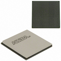
EP3SL150F1152C3N Altera, EP3SL150F1152C3N Datasheet - Page 247

EP3SL150F1152C3N
Manufacturer Part Number
EP3SL150F1152C3N
Description
IC STRATX III FPGA 150K 1152FBGA
Manufacturer
Altera
Series
Stratix® IIIr
Datasheets
1.EP3SL150F780C4N.pdf
(16 pages)
2.EP3SL150F780C4N.pdf
(332 pages)
3.EP3SL150F780C4N.pdf
(456 pages)
Specifications of EP3SL150F1152C3N
Number Of Logic Elements/cells
142500
Number Of Labs/clbs
5700
Total Ram Bits
6390
Number Of I /o
744
Voltage - Supply
0.86 V ~ 1.15 V
Mounting Type
Surface Mount
Operating Temperature
0°C ~ 85°C
Package / Case
1152-FBGA
For Use With
544-2568 - KIT DEVELOPMENT STRATIX III
Lead Free Status / RoHS Status
Lead free / RoHS Compliant
Number Of Gates
-
Other names
544-2408
EP3SL150F1152C3NES
EP3SL150F1152C3NES
Available stocks
Company
Part Number
Manufacturer
Quantity
Price
Company:
Part Number:
EP3SL150F1152C3N
Manufacturer:
ALTERA
Quantity:
490
- Current page: 247 of 456
- Download datasheet (7Mb)
Chapter 7: Stratix III Device I/O Features
Chapter Revision History
Table 7–13. Chapter Revision History (Part 2 of 2)
© July 2010
May 2008
November 2007
October 2007
May 2007
November 2006
Date and Revision
Altera Corporation
Version
1.4
1.3
1.2
1.1
1.0
Text, Table, and Figure updates:
■
■
■
■
■
■
■
Figure updates:
■
■
Text changes, figure updates, removal of a section:
■
■
■
■
■
■
■
■
■
■
■
■
■
■
■
■
■
Initial Release.
Updated Table 7–2 headers and notes.
Updated Figure 7–1.
Updated “Programmable Slew Rate Control”, “Programmable
Pre-Emphasis”, “LVDS Input On-Chip Termination (RD)”, and
“Programmable Differential Output Voltage”.
Added Note (1) for Figure 7–17.
Updated notes for Figure 7–24.
Added Note (2) for Figure 7–27.
Added Note (2) for Figure 7–28.
Updated Figure 7–4, Figure 7–5, Figure 7–6, Figure 7–15, and
Figure 7–16.
Updated Note (1) of Figure 7–25.
Minor text edits to second to last paragraph on pg 7-47.
Updated Table 7–2, Table 7–4, Table 7–5, Table 7–8.
Updated “Introduction”, “OCT Calibration Block Modes of Operation”,
“Power Up Mode”, “User Mode”.
Changed 3.0-V LVTTL and 3.0-V LVCMOS to be 3.3/3.0-V LVTTL and
3.3/3.0-V LVCMOS throughout the document.
Added a note to Figure 7–1, Figure 7–3, Figure 7–4, Figure 7–5,
Figure 7–6, Figure 7–7, Figure 7–14, Figure 7–15, Figure 7–16, and
Figure 7–17.
Updated Figure 7–8, Figure 7–18, Figure 7–22, Figure 7–23,
Figure 7–25, Figure 7–28, and Figure 7–29.
Added Figure 7–18 and Figure 7–20.
Expanded “3.3-V I/O Interface” on page 7–15 to include new
information.
Removed section “OCT Calibration Block Architecture”, “OCT Calibration
Block Ports”, and “OCT Calibration Block Code Data Transfer”.
Added section “OCT Calibration”, “Serial Data Transfer”, “Example of
Using Multiple OCT Calibration Blocks”, “RS Calibration”, and
“Referenced Documents.”
Added live links for references.
Added the feature programmable input delay to “Stratix III I/O
Structure” on page 7–13.
Updated Table 7–4 and Table 7–7.
Updated “LVDS Input On-Chip Termination (RD)” on page 7–29.
Updated Figure 7–3 through Figure 7–7.
Updated Figure 7–23, Figure 7–24.
Minor text edits to page 14.
Changes Made
Stratix III Device Handbook, Volume 1
7–43
Related parts for EP3SL150F1152C3N
Image
Part Number
Description
Manufacturer
Datasheet
Request
R

Part Number:
Description:
CYCLONE II STARTER KIT EP2C20N
Manufacturer:
Altera
Datasheet:

Part Number:
Description:
CPLD, EP610 Family, ECMOS Process, 300 Gates, 16 Macro Cells, 16 Reg., 16 User I/Os, 5V Supply, 35 Speed Grade, 24DIP
Manufacturer:
Altera Corporation
Datasheet:

Part Number:
Description:
CPLD, EP610 Family, ECMOS Process, 300 Gates, 16 Macro Cells, 16 Reg., 16 User I/Os, 5V Supply, 15 Speed Grade, 24DIP
Manufacturer:
Altera Corporation
Datasheet:

Part Number:
Description:
Manufacturer:
Altera Corporation
Datasheet:

Part Number:
Description:
CPLD, EP610 Family, ECMOS Process, 300 Gates, 16 Macro Cells, 16 Reg., 16 User I/Os, 5V Supply, 30 Speed Grade, 24DIP
Manufacturer:
Altera Corporation
Datasheet:

Part Number:
Description:
High-performance, low-power erasable programmable logic devices with 8 macrocells, 10ns
Manufacturer:
Altera Corporation
Datasheet:

Part Number:
Description:
High-performance, low-power erasable programmable logic devices with 8 macrocells, 7ns
Manufacturer:
Altera Corporation
Datasheet:

Part Number:
Description:
Classic EPLD
Manufacturer:
Altera Corporation
Datasheet:

Part Number:
Description:
High-performance, low-power erasable programmable logic devices with 8 macrocells, 10ns
Manufacturer:
Altera Corporation
Datasheet:

Part Number:
Description:
Manufacturer:
Altera Corporation
Datasheet:

Part Number:
Description:
Manufacturer:
Altera Corporation
Datasheet:

Part Number:
Description:
Manufacturer:
Altera Corporation
Datasheet:

Part Number:
Description:
CPLD, EP610 Family, ECMOS Process, 300 Gates, 16 Macro Cells, 16 Reg., 16 User I/Os, 5V Supply, 25 Speed Grade, 24DIP
Manufacturer:
Altera Corporation
Datasheet:


