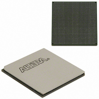
EP3SL150F1152C3N Altera, EP3SL150F1152C3N Datasheet - Page 262

EP3SL150F1152C3N
Manufacturer Part Number
EP3SL150F1152C3N
Description
IC STRATX III FPGA 150K 1152FBGA
Manufacturer
Altera
Series
Stratix® IIIr
Datasheets
1.EP3SL150F780C4N.pdf
(16 pages)
2.EP3SL150F780C4N.pdf
(332 pages)
3.EP3SL150F780C4N.pdf
(456 pages)
Specifications of EP3SL150F1152C3N
Number Of Logic Elements/cells
142500
Number Of Labs/clbs
5700
Total Ram Bits
6390
Number Of I /o
744
Voltage - Supply
0.86 V ~ 1.15 V
Mounting Type
Surface Mount
Operating Temperature
0°C ~ 85°C
Package / Case
1152-FBGA
For Use With
544-2568 - KIT DEVELOPMENT STRATIX III
Lead Free Status / RoHS Status
Lead free / RoHS Compliant
Number Of Gates
-
Other names
544-2408
EP3SL150F1152C3NES
EP3SL150F1152C3NES
Available stocks
Company
Part Number
Manufacturer
Quantity
Price
Company:
Part Number:
EP3SL150F1152C3N
Manufacturer:
ALTERA
Quantity:
490
- Current page: 262 of 456
- Download datasheet (7Mb)
8–14
Figure 8–8. DQS Pins in Stratix III I/O Banks
Stratix III Device Handbook, Volume 1
DQS20L
DQS21L
DQS40L
PLL_L4
PLL_L1
DQS1L
PLL_L2
PLL_L3
DLL1
DLL0
1A
1C
2B
1B
2C
2A
DQS44T
DQS1B
8A
3A
DQ pin numbering is based on ×4 mode. In ×4 mode, there are up to eight DQS/DQ
groups per I/O bank. Each ×4 mode DQS/DQ group consists of a DQS pin, a DQSn
pin, and four DQ pins. In ×8/×9 mode, the I/O bank combines two adjacent ×4
DQS/DQ groups; one pair of DQS and DQSn/CQn pins can drive all the DQ and
parity pins in the new combined group that consists of up to 10 DQ pins (including
parity or DM and QVLD pins) and a pair of DQS and DQSn/CQn pins.
8B
3B
8C
3C
DQS23T
DQS22B
Stratix III Device
PLL_T1
PLL_B1
PLL_T2
PLL_B2
Chapter 8: External Memory Interfaces in Stratix III Devices
DQS22T
DQS23B
7C
4C
7B
4B
© March 2010 Altera Corporation
Memory Interfaces Pin Support
7A
4A
DQS44B
DQS1T
6A
6B
6C
5C
5A
5B
DLL3
DLL2
PLL_R2
PLL_R3
DQS40R
DQS21R
DQS20R
DQS1R
PLL_R4
PLL_R1
Related parts for EP3SL150F1152C3N
Image
Part Number
Description
Manufacturer
Datasheet
Request
R

Part Number:
Description:
CYCLONE II STARTER KIT EP2C20N
Manufacturer:
Altera
Datasheet:

Part Number:
Description:
CPLD, EP610 Family, ECMOS Process, 300 Gates, 16 Macro Cells, 16 Reg., 16 User I/Os, 5V Supply, 35 Speed Grade, 24DIP
Manufacturer:
Altera Corporation
Datasheet:

Part Number:
Description:
CPLD, EP610 Family, ECMOS Process, 300 Gates, 16 Macro Cells, 16 Reg., 16 User I/Os, 5V Supply, 15 Speed Grade, 24DIP
Manufacturer:
Altera Corporation
Datasheet:

Part Number:
Description:
Manufacturer:
Altera Corporation
Datasheet:

Part Number:
Description:
CPLD, EP610 Family, ECMOS Process, 300 Gates, 16 Macro Cells, 16 Reg., 16 User I/Os, 5V Supply, 30 Speed Grade, 24DIP
Manufacturer:
Altera Corporation
Datasheet:

Part Number:
Description:
High-performance, low-power erasable programmable logic devices with 8 macrocells, 10ns
Manufacturer:
Altera Corporation
Datasheet:

Part Number:
Description:
High-performance, low-power erasable programmable logic devices with 8 macrocells, 7ns
Manufacturer:
Altera Corporation
Datasheet:

Part Number:
Description:
Classic EPLD
Manufacturer:
Altera Corporation
Datasheet:

Part Number:
Description:
High-performance, low-power erasable programmable logic devices with 8 macrocells, 10ns
Manufacturer:
Altera Corporation
Datasheet:

Part Number:
Description:
Manufacturer:
Altera Corporation
Datasheet:

Part Number:
Description:
Manufacturer:
Altera Corporation
Datasheet:

Part Number:
Description:
Manufacturer:
Altera Corporation
Datasheet:

Part Number:
Description:
CPLD, EP610 Family, ECMOS Process, 300 Gates, 16 Macro Cells, 16 Reg., 16 User I/Os, 5V Supply, 25 Speed Grade, 24DIP
Manufacturer:
Altera Corporation
Datasheet:


