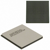
EP3SL150F1152C3N Altera, EP3SL150F1152C3N Datasheet - Page 266

EP3SL150F1152C3N
Manufacturer Part Number
EP3SL150F1152C3N
Description
IC STRATX III FPGA 150K 1152FBGA
Manufacturer
Altera
Series
Stratix® IIIr
Datasheets
1.EP3SL150F780C4N.pdf
(16 pages)
2.EP3SL150F780C4N.pdf
(332 pages)
3.EP3SL150F780C4N.pdf
(456 pages)
Specifications of EP3SL150F1152C3N
Number Of Logic Elements/cells
142500
Number Of Labs/clbs
5700
Total Ram Bits
6390
Number Of I /o
744
Voltage - Supply
0.86 V ~ 1.15 V
Mounting Type
Surface Mount
Operating Temperature
0°C ~ 85°C
Package / Case
1152-FBGA
For Use With
544-2568 - KIT DEVELOPMENT STRATIX III
Lead Free Status / RoHS Status
Lead free / RoHS Compliant
Number Of Gates
-
Other names
544-2408
EP3SL150F1152C3NES
EP3SL150F1152C3NES
Available stocks
Company
Part Number
Manufacturer
Quantity
Price
Company:
Part Number:
EP3SL150F1152C3N
Manufacturer:
ALTERA
Quantity:
490
- Current page: 266 of 456
- Download datasheet (7Mb)
8–18
Memory Clock Pins
Figure 8–9. Memory Clock Generation Block Diagram
Notes to
(1) For more information about pin location requirements for these pins, refer
(2) The mem_clk[0] and mem_clk_n[0] pins for DDR3, DDR2, and DDR SDRAM interfaces use the I/O input buffer for feedback; therefore,
Stratix III External Memory Interface Features
Stratix III Device Handbook, Volume 1
Memory Interface Handbook.
bi-directional I/O buffers are used for these pins. For memory interfaces using a differential DQS input, the input feedback buffer is configured as
differential input; for memory interfaces using a single-ended DQS input, the input buffer is configured as a single-ended input. Using a
single-ended input feedback buffer requires that I/O standard’s V
Figure
System Clock
f
8–9:
In addition to DQS (and CQn) signals to capture data, DDR3, DDR2, DDR SDRAM,
and RLDRAM II use an extra pair of clocks, called CK and CK# signals, to capture the
address and control/command signals. The CK/CK# signals must be generated to
mimic the write data-strobe using Stratix III DDR I/O registers (DDIOs) to ensure that
timing relationships between the CK/CK# and DQS signals (t
DDR SDRAM or t
use the same clock (K/K#) to capture data, address, and control/command signals.
Memory clock pins in Stratix III devices are generated with a DDIO register going to
differential output pins, marked in the pin table with DIFFOUT, DIFFIO_TX, and
DIFFIO_RX prefixes.
For more information about which pins to use for memory clock pins, refer to the
Section I. Device and Pin Planning
Handbook.
Figure 8–9
Stratix III devices are rich with features that allow robust high-performance external
memory interfacing. The ALTMEMPHY megafunction allows you to set these
external memory interface features and helps set up the physical interface (PHY) best
suited for your system. This section describes each Stratix III device feature that is
used in external memory interfaces from the DQS phase-shift circuitry, DQS logic
block, leveling multiplexers, dynamic OCT control block, IOE registers, IOE features,
and PLLs.
V CC
shows the memory clock generation block diagram for Stratix III devices.
FPGA LEs
CKDK
in RLDRAM II) are met. QDR II+ and QDR II SRAM devices
I/O Elements
(Note 1)
REF
voltage is provided to that I/O bank’s VREF pins.
chapter in volume 2 of the External Memory Interface
D
D
Section I. Device and Pin Planning
Q
Q
Chapter 8: External Memory Interfaces in Stratix III Devices
Stratix III External Memory Interface Features
© March 2010 Altera Corporation
chapter in volume 2 of the External
DQSS
CK or DK or K (2)
CK# or DK# or K# (2)
in DDR3, DDR2, and
Related parts for EP3SL150F1152C3N
Image
Part Number
Description
Manufacturer
Datasheet
Request
R

Part Number:
Description:
CYCLONE II STARTER KIT EP2C20N
Manufacturer:
Altera
Datasheet:

Part Number:
Description:
CPLD, EP610 Family, ECMOS Process, 300 Gates, 16 Macro Cells, 16 Reg., 16 User I/Os, 5V Supply, 35 Speed Grade, 24DIP
Manufacturer:
Altera Corporation
Datasheet:

Part Number:
Description:
CPLD, EP610 Family, ECMOS Process, 300 Gates, 16 Macro Cells, 16 Reg., 16 User I/Os, 5V Supply, 15 Speed Grade, 24DIP
Manufacturer:
Altera Corporation
Datasheet:

Part Number:
Description:
Manufacturer:
Altera Corporation
Datasheet:

Part Number:
Description:
CPLD, EP610 Family, ECMOS Process, 300 Gates, 16 Macro Cells, 16 Reg., 16 User I/Os, 5V Supply, 30 Speed Grade, 24DIP
Manufacturer:
Altera Corporation
Datasheet:

Part Number:
Description:
High-performance, low-power erasable programmable logic devices with 8 macrocells, 10ns
Manufacturer:
Altera Corporation
Datasheet:

Part Number:
Description:
High-performance, low-power erasable programmable logic devices with 8 macrocells, 7ns
Manufacturer:
Altera Corporation
Datasheet:

Part Number:
Description:
Classic EPLD
Manufacturer:
Altera Corporation
Datasheet:

Part Number:
Description:
High-performance, low-power erasable programmable logic devices with 8 macrocells, 10ns
Manufacturer:
Altera Corporation
Datasheet:

Part Number:
Description:
Manufacturer:
Altera Corporation
Datasheet:

Part Number:
Description:
Manufacturer:
Altera Corporation
Datasheet:

Part Number:
Description:
Manufacturer:
Altera Corporation
Datasheet:

Part Number:
Description:
CPLD, EP610 Family, ECMOS Process, 300 Gates, 16 Macro Cells, 16 Reg., 16 User I/Os, 5V Supply, 25 Speed Grade, 24DIP
Manufacturer:
Altera Corporation
Datasheet:


