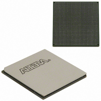
EP3SL150F1152C3N Altera, EP3SL150F1152C3N Datasheet - Page 274

EP3SL150F1152C3N
Manufacturer Part Number
EP3SL150F1152C3N
Description
IC STRATX III FPGA 150K 1152FBGA
Manufacturer
Altera
Series
Stratix® IIIr
Datasheets
1.EP3SL150F780C4N.pdf
(16 pages)
2.EP3SL150F780C4N.pdf
(332 pages)
3.EP3SL150F780C4N.pdf
(456 pages)
Specifications of EP3SL150F1152C3N
Number Of Logic Elements/cells
142500
Number Of Labs/clbs
5700
Total Ram Bits
6390
Number Of I /o
744
Voltage - Supply
0.86 V ~ 1.15 V
Mounting Type
Surface Mount
Operating Temperature
0°C ~ 85°C
Package / Case
1152-FBGA
For Use With
544-2568 - KIT DEVELOPMENT STRATIX III
Lead Free Status / RoHS Status
Lead free / RoHS Compliant
Number Of Gates
-
Other names
544-2408
EP3SL150F1152C3NES
EP3SL150F1152C3NES
Available stocks
Company
Part Number
Manufacturer
Quantity
Price
Company:
Part Number:
EP3SL150F1152C3N
Manufacturer:
ALTERA
Quantity:
490
- Current page: 274 of 456
- Download datasheet (7Mb)
8–26
Figure 8–12. Simplified Diagram of the DQS Phase Shift Circuitry
Notes to
(1) All features of the DQS phase-shift circuitry are accessible from the ALTMEMPHY megafunction in the Quartus II software.
(2) The input reference clock for the DQS phase-shift circuitry can come from a PLL output clock or an input clock pin. For the exact PLL and input
(3) Phase offset settings can only go to the DQS logic blocks.
(4) DQS delay settings can go to the logic array, the DQS logic block, and the leveling circuitry.
Stratix III Device Handbook, Volume 1
clock pin location, refer to
Input Reference
Figure
Clock (2)
8–12:
1
clk
DLL
The phase offset control block ‘A’ is designated as
DLLOFFSETCTRL_<coordinate x>_<coordinate y>_N1 and phase offset
control block ‘B’ is designated as
DLLOFFSETCTRL_<coordinate x>_<coordinate y>_N2 in the Quartus II
assignment.
You can reset the DLL from either the logic array or a user I/O pin. Each time the DLL
is reset, you must wait for 1280 clock cycles before you can capture the data properly.
Depending on the DLL frequency mode, the DLL can shift the incoming DQS signals
by 0°, 22.5°, 30°, 36°, 45°, 60°, 67.5°, 72°, 90°, 108°, 120°, 135°, 144°, or 180°. The shifted
DQS signal is then used as the clock for the DQ IOE input registers.
All DQS and CQn pins referenced to the same DLL can have their input signal phase
shifted by a different degree amount but all must be referenced at one particular
frequency. For example, you can have a 90° phase shift on DQS1T and a 60° phase shift
on DQS2T referenced from a 200-MHz clock. Not all phase-shift combinations are
supported, however. The phase shifts on the DQS pins referenced by the same DLL
must all be a multiple of 22.5° (up to 90°), a multiple of 30° (up to 120°), a multiple
of 36° (up to 144°), or a multiple of 45° (up to 180°).
There are seven different frequency modes for the Stratix III DLL, as listed in
Table
frequency modes 0, 1, 2, and 3, the 6-bit DQS delay settings vary with PVT to
implement the phase-shift delay. In frequency modes 4, 5, 6, and 7, only 5 bits of the
DQS delay settings vary with PVT to implement a phase-shift delay; the most
significant bit of the DQS delay setting is set to 0.
Comparator
aload
Table 8–6
Phase
8–10. Each frequency mode provides different phase shift selections. In
Delay Chains
upndninclkena
through
upndnin
Table
Up/Down
Counter
8–9.
6
6
offsetdelayctrlout [5:0]
offsetdelayctrlout [5:0]
delayctrlout [5:0]
dqsupdate
(Note 1)
Chapter 8: External Memory Interfaces in Stratix III Devices
offsetdelayctrlin [5:0]
offsetdelayctrlin [5:0]
6
DQS Delay
Settings
addnsub
addnsub
Stratix III External Memory Interface Features
Phase offset settings
from the logic array
Phase offset settings
from the logic array
( offset [5:0] )
(4)
6
6
(dll_offset_ctrl_b)
(dll_offset_ctrl_a)
© March 2010 Altera Corporation
Control
Control
Phase
Phase
Offset
Offset
B
A
( offset [5:0] )
6
6
Phase offset
settings to DQS pin
on left or right edge (3)
( offsetctrlout [5:0] )
Phase offset
settings to DQS pins
on top or bottom edge (3)
( offsetctrlout [5:0] )
Related parts for EP3SL150F1152C3N
Image
Part Number
Description
Manufacturer
Datasheet
Request
R

Part Number:
Description:
CYCLONE II STARTER KIT EP2C20N
Manufacturer:
Altera
Datasheet:

Part Number:
Description:
CPLD, EP610 Family, ECMOS Process, 300 Gates, 16 Macro Cells, 16 Reg., 16 User I/Os, 5V Supply, 35 Speed Grade, 24DIP
Manufacturer:
Altera Corporation
Datasheet:

Part Number:
Description:
CPLD, EP610 Family, ECMOS Process, 300 Gates, 16 Macro Cells, 16 Reg., 16 User I/Os, 5V Supply, 15 Speed Grade, 24DIP
Manufacturer:
Altera Corporation
Datasheet:

Part Number:
Description:
Manufacturer:
Altera Corporation
Datasheet:

Part Number:
Description:
CPLD, EP610 Family, ECMOS Process, 300 Gates, 16 Macro Cells, 16 Reg., 16 User I/Os, 5V Supply, 30 Speed Grade, 24DIP
Manufacturer:
Altera Corporation
Datasheet:

Part Number:
Description:
High-performance, low-power erasable programmable logic devices with 8 macrocells, 10ns
Manufacturer:
Altera Corporation
Datasheet:

Part Number:
Description:
High-performance, low-power erasable programmable logic devices with 8 macrocells, 7ns
Manufacturer:
Altera Corporation
Datasheet:

Part Number:
Description:
Classic EPLD
Manufacturer:
Altera Corporation
Datasheet:

Part Number:
Description:
High-performance, low-power erasable programmable logic devices with 8 macrocells, 10ns
Manufacturer:
Altera Corporation
Datasheet:

Part Number:
Description:
Manufacturer:
Altera Corporation
Datasheet:

Part Number:
Description:
Manufacturer:
Altera Corporation
Datasheet:

Part Number:
Description:
Manufacturer:
Altera Corporation
Datasheet:

Part Number:
Description:
CPLD, EP610 Family, ECMOS Process, 300 Gates, 16 Macro Cells, 16 Reg., 16 User I/Os, 5V Supply, 25 Speed Grade, 24DIP
Manufacturer:
Altera Corporation
Datasheet:


