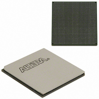
EP3SL150F1152C3N Altera, EP3SL150F1152C3N Datasheet - Page 296

EP3SL150F1152C3N
Manufacturer Part Number
EP3SL150F1152C3N
Description
IC STRATX III FPGA 150K 1152FBGA
Manufacturer
Altera
Series
Stratix® IIIr
Datasheets
1.EP3SL150F780C4N.pdf
(16 pages)
2.EP3SL150F780C4N.pdf
(332 pages)
3.EP3SL150F780C4N.pdf
(456 pages)
Specifications of EP3SL150F1152C3N
Number Of Logic Elements/cells
142500
Number Of Labs/clbs
5700
Total Ram Bits
6390
Number Of I /o
744
Voltage - Supply
0.86 V ~ 1.15 V
Mounting Type
Surface Mount
Operating Temperature
0°C ~ 85°C
Package / Case
1152-FBGA
For Use With
544-2568 - KIT DEVELOPMENT STRATIX III
Lead Free Status / RoHS Status
Lead free / RoHS Compliant
Number Of Gates
-
Other names
544-2408
EP3SL150F1152C3NES
EP3SL150F1152C3NES
Available stocks
Company
Part Number
Manufacturer
Quantity
Price
Company:
Part Number:
EP3SL150F1152C3N
Manufacturer:
ALTERA
Quantity:
490
- Current page: 296 of 456
- Download datasheet (7Mb)
9–2
I/O Banks
Figure 9–1. I/O Banks in Stratix III Devices
Notes to
(1)
(2) Differential HSTL and SSTL outputs use two single-ended (SE) outputs with the second output programmed as inverted to support differential I/O
(3) Column I/O differential HSTL and SSTL inputs use LVDS differential input buffers without on-chip differential termination (OCT R
(4) Column I/O supports LVDS outputs using SE buffers and external resistor networks.
(5) Row I/O supports PCI/PCI-X without on-chip clamping diodes.
(6) The PLL blocks are shown for location purposes only and are not considered additional banks. The PLL input and output uses the I/Os in adjacent
Stratix III Device Handbook, Volume 1
Figure 9–1
locations, refer to the pin list and the Quartus II software.
operations.
banks.
PLL_L2
PLL_L1
PLL_L3
PLL_L4
Figure
Stratix III I/O Banks
is a top view of the silicon die that corresponds to a reverse view for flip chip packages. It is a graphical representation only. For exact
9–1:
Bank 8A
Bank 3A
I/O banks 3A, 3B & 3C support all
single-ended and differential input
and output operation
Stratix III I/Os are divided into 16 to 24 I/O banks. The dedicated serializer and
deserializer (SERDES) circuitry with DPA that supports high-speed differential I/Os
is located in banks in the right side and left side of the device.
different banks and the I/O standards supported by the banks.
I/O banks 8A, 8B & 8C support all
single-ended and differential input
and output operation
Bank 3B
Bank 8B
Row I/O banks support LVTTL, LVCMOS, 2.5-V, 1.8-V,
1.5-V, 1.2-V, SSTL-2 Class I & II, SSTL-18 Class I & II,
SSTL-15 Class I, HSTL-18 Class I & II, HSTL-15 Class I,
HSTL-12 Class I, LVDS, RSDS, mini-LVDS, differential
SSTL-2 Class I & II, differential SSTL-18 Class I & II,
differential SSTL-15 Class I, differential HSTL-18 Class I &
II, differential HSTL-15 Class I and differential HSTL-12
Class I standards for input and output operation.
SSTL-15 class II, HSTL-15 Class II, HSTL-12 Class II,
differential SSTL-15 Class II, differential HSTL-15 Class II,
differential HSTL-12 Class II standards are only supported
for input operations
Bank 3C
Bank 8C
(Note
1), (2), (3), (4), (5),
PLL_B1 PLL_B2
PLL_T1
Chapter 9: High-Speed Differential I/O Interfaces and DPA in Stratix III Devices
PLL_T2
(6)
Bank 4C
Bank 7C
I/O banks 4A, 4B & 4C support all
single-ended and differential input
and output operation
I/O banks 7A, 7B & 7C support all
single-ended and differential input
and output operation
Bank 4B
Bank 7B
© July 2010 Altera Corporation
Figure 9–1
Bank 4A
Bank 7A
shows the
PLL_R2
PLL_R3
PLL_R4
PLL_R1
D
) support.
I/O Banks
Related parts for EP3SL150F1152C3N
Image
Part Number
Description
Manufacturer
Datasheet
Request
R

Part Number:
Description:
CYCLONE II STARTER KIT EP2C20N
Manufacturer:
Altera
Datasheet:

Part Number:
Description:
CPLD, EP610 Family, ECMOS Process, 300 Gates, 16 Macro Cells, 16 Reg., 16 User I/Os, 5V Supply, 35 Speed Grade, 24DIP
Manufacturer:
Altera Corporation
Datasheet:

Part Number:
Description:
CPLD, EP610 Family, ECMOS Process, 300 Gates, 16 Macro Cells, 16 Reg., 16 User I/Os, 5V Supply, 15 Speed Grade, 24DIP
Manufacturer:
Altera Corporation
Datasheet:

Part Number:
Description:
Manufacturer:
Altera Corporation
Datasheet:

Part Number:
Description:
CPLD, EP610 Family, ECMOS Process, 300 Gates, 16 Macro Cells, 16 Reg., 16 User I/Os, 5V Supply, 30 Speed Grade, 24DIP
Manufacturer:
Altera Corporation
Datasheet:

Part Number:
Description:
High-performance, low-power erasable programmable logic devices with 8 macrocells, 10ns
Manufacturer:
Altera Corporation
Datasheet:

Part Number:
Description:
High-performance, low-power erasable programmable logic devices with 8 macrocells, 7ns
Manufacturer:
Altera Corporation
Datasheet:

Part Number:
Description:
Classic EPLD
Manufacturer:
Altera Corporation
Datasheet:

Part Number:
Description:
High-performance, low-power erasable programmable logic devices with 8 macrocells, 10ns
Manufacturer:
Altera Corporation
Datasheet:

Part Number:
Description:
Manufacturer:
Altera Corporation
Datasheet:

Part Number:
Description:
Manufacturer:
Altera Corporation
Datasheet:

Part Number:
Description:
Manufacturer:
Altera Corporation
Datasheet:

Part Number:
Description:
CPLD, EP610 Family, ECMOS Process, 300 Gates, 16 Macro Cells, 16 Reg., 16 User I/Os, 5V Supply, 25 Speed Grade, 24DIP
Manufacturer:
Altera Corporation
Datasheet:


