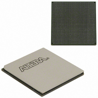
EP3SL150F1152C3N Altera, EP3SL150F1152C3N Datasheet - Page 298

EP3SL150F1152C3N
Manufacturer Part Number
EP3SL150F1152C3N
Description
IC STRATX III FPGA 150K 1152FBGA
Manufacturer
Altera
Series
Stratix® IIIr
Datasheets
1.EP3SL150F780C4N.pdf
(16 pages)
2.EP3SL150F780C4N.pdf
(332 pages)
3.EP3SL150F780C4N.pdf
(456 pages)
Specifications of EP3SL150F1152C3N
Number Of Logic Elements/cells
142500
Number Of Labs/clbs
5700
Total Ram Bits
6390
Number Of I /o
744
Voltage - Supply
0.86 V ~ 1.15 V
Mounting Type
Surface Mount
Operating Temperature
0°C ~ 85°C
Package / Case
1152-FBGA
For Use With
544-2568 - KIT DEVELOPMENT STRATIX III
Lead Free Status / RoHS Status
Lead free / RoHS Compliant
Number Of Gates
-
Other names
544-2408
EP3SL150F1152C3NES
EP3SL150F1152C3NES
Available stocks
Company
Part Number
Manufacturer
Quantity
Price
Company:
Part Number:
EP3SL150F1152C3N
Manufacturer:
ALTERA
Quantity:
490
- Current page: 298 of 456
- Download datasheet (7Mb)
9–4
Table 9–2. LVDS Channels (Emulated) Supported in Stratix III Device Column I/O Banks
Differential Transmitter
Stratix III Device Handbook, Volume 1
EP3SL50
EP3SL70
EP3SL110
EP3SL150
EP3SL200
EP3SL340
EP3SE50
EP3SE80
EP3SE110
EP3SE260
Notes to
(1) Rx = true LVDS input buffers without on-chip differential input termination.
(2) eTx = emulated LVDS output buffers, either LVDS_E3R or LVDS_E1R.
(3) The EP3SL200 and EP3SE260 FPGAs are offered in the H780 package, instead of the F780 package.
(4) The EP3SL340 FPGA is offered in the H1152 package, instead of the F1152 package.
Device
Table
24Rx/eTx + 24eTx
24Rx/eTx + 24eTx
24Rx/eTx + 24eTx
484-Pin FineLine
9–2:
BGA
—
—
—
—
—
—
—
Table 9–2
I/O banks.
The Stratix III transmitter has dedicated circuitry to provide support for LVDS
signaling. The dedicated circuitry consists of a differential buffer, a serializer, and a
shared analog PLL (left/right PLL). The differential buffer can drive out LVDS,
mini-LVDS, and RSDS signaling levels. The serializer takes up to 10-bits wide parallel
data from the FPGA core, clocks it into the load registers, and serializes it using shift
registers clocked by the left/right PLL before sending the data to the differential
buffer. The most significant bit (MSB) of the parallel data is transmitted first.
The load and shift registers are clocked by the load enable (load_en) signal and the
diffioclk (clock running at serial data rate) signal generated from PLL_Lx (left
PLL) or PLL_Rx (right PLL). The serialization factor can be statically set to ×3, ×4, ×5,
×6, ×7, ×8, ×9, or ×10 with the Quartus II software. The load enable signal is derived
from the serialization factor setting.
Stratix III transmitter.
64Rx/eTx + 64eTx
64Rx/eTx + 64eTx
lists the LVDS channels (emulated) supported in Stratix III device column
64Rx/eTx + 64eTx
64Rx/eTx + 64eTx
64Rx/eTx + 64eTx
64Rx/eTx + 64eTx
64Rx/eTx + 64eTx
64Rx/eTx + 64eTx
64Rx/eTx + 64eTx
FineLine BGA
780-Pin
—
(3)
(3)
Chapter 9: High-Speed Differential I/O Interfaces and DPA in Stratix III Devices
96Rx/eTx + 96eTx
96Rx/eTx + 96eTx
96Rx/eTx + 96eTx
96Rx/eTx + 96eTx
96Rx/eTx + 96eTx
96Rx/eTx + 96eTx
96Rx/eTx + 96eTx
FineLine BGA
1152-Pin
Figure 9–2
—
—
—
(4)
shows a block diagram of the
128Rx/eTx + 128eTx
128Rx/eTx + 128eTx 144Rx/eTx + 144eTx
128Rx/eTx + 128eTx
1517-Pin FineLine
(Note
BGA
—
—
—
—
—
—
—
1),
© July 2010 Altera Corporation
(2)
Differential Transmitter
1780-Pin FineLine
BGA
—
—
—
—
—
—
—
—
—
Related parts for EP3SL150F1152C3N
Image
Part Number
Description
Manufacturer
Datasheet
Request
R

Part Number:
Description:
CYCLONE II STARTER KIT EP2C20N
Manufacturer:
Altera
Datasheet:

Part Number:
Description:
CPLD, EP610 Family, ECMOS Process, 300 Gates, 16 Macro Cells, 16 Reg., 16 User I/Os, 5V Supply, 35 Speed Grade, 24DIP
Manufacturer:
Altera Corporation
Datasheet:

Part Number:
Description:
CPLD, EP610 Family, ECMOS Process, 300 Gates, 16 Macro Cells, 16 Reg., 16 User I/Os, 5V Supply, 15 Speed Grade, 24DIP
Manufacturer:
Altera Corporation
Datasheet:

Part Number:
Description:
Manufacturer:
Altera Corporation
Datasheet:

Part Number:
Description:
CPLD, EP610 Family, ECMOS Process, 300 Gates, 16 Macro Cells, 16 Reg., 16 User I/Os, 5V Supply, 30 Speed Grade, 24DIP
Manufacturer:
Altera Corporation
Datasheet:

Part Number:
Description:
High-performance, low-power erasable programmable logic devices with 8 macrocells, 10ns
Manufacturer:
Altera Corporation
Datasheet:

Part Number:
Description:
High-performance, low-power erasable programmable logic devices with 8 macrocells, 7ns
Manufacturer:
Altera Corporation
Datasheet:

Part Number:
Description:
Classic EPLD
Manufacturer:
Altera Corporation
Datasheet:

Part Number:
Description:
High-performance, low-power erasable programmable logic devices with 8 macrocells, 10ns
Manufacturer:
Altera Corporation
Datasheet:

Part Number:
Description:
Manufacturer:
Altera Corporation
Datasheet:

Part Number:
Description:
Manufacturer:
Altera Corporation
Datasheet:

Part Number:
Description:
Manufacturer:
Altera Corporation
Datasheet:

Part Number:
Description:
CPLD, EP610 Family, ECMOS Process, 300 Gates, 16 Macro Cells, 16 Reg., 16 User I/Os, 5V Supply, 25 Speed Grade, 24DIP
Manufacturer:
Altera Corporation
Datasheet:


