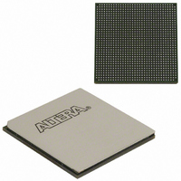
EP3SL150F1152C3N Altera, EP3SL150F1152C3N Datasheet - Page 303

EP3SL150F1152C3N
Manufacturer Part Number
EP3SL150F1152C3N
Description
IC STRATX III FPGA 150K 1152FBGA
Manufacturer
Altera
Series
Stratix® IIIr
Datasheets
1.EP3SL150F780C4N.pdf
(16 pages)
2.EP3SL150F780C4N.pdf
(332 pages)
3.EP3SL150F780C4N.pdf
(456 pages)
Specifications of EP3SL150F1152C3N
Number Of Logic Elements/cells
142500
Number Of Labs/clbs
5700
Total Ram Bits
6390
Number Of I /o
744
Voltage - Supply
0.86 V ~ 1.15 V
Mounting Type
Surface Mount
Operating Temperature
0°C ~ 85°C
Package / Case
1152-FBGA
For Use With
544-2568 - KIT DEVELOPMENT STRATIX III
Lead Free Status / RoHS Status
Lead free / RoHS Compliant
Number Of Gates
-
Other names
544-2408
EP3SL150F1152C3NES
EP3SL150F1152C3NES
Available stocks
Company
Part Number
Manufacturer
Quantity
Price
Company:
Part Number:
EP3SL150F1152C3N
Manufacturer:
ALTERA
Quantity:
490
- Current page: 303 of 456
- Download datasheet (7Mb)
Chapter 9: High-Speed Differential I/O Interfaces and DPA in Stratix III Devices
Differential Receiver
Soft-CDR Mode
© July 2010
Altera Corporation
1
The DPA circuitry does not require a fixed training pattern to lock to the optimum
phase out of the 8 phases. After reset or power up, the DPA circuitry requires
transitions on the received data to lock to the optimum phase. The ALTLVDS
megafunction provides an optional output port, rx_dpa_locked to indicate if the
DPA has locked to the optimum phase. When the DPA locks to the optimum phase,
the rx_dpa_locked signal always stays high unless you assert the rx_reset signal
of the associated LVDS channel or the pll_areset signal of the receiver PLL
providing the 8 DPA clock phases.
The rx_dpa_locked signal only indicates an initial DPA lock condition to the
optimum phase after power up or reset. You must not use the rx_dpa_locked signal
to validate the integrity of the LVDS link. Use error checkers, for example cyclical
redundancy check (CRC) and diagonal interleave parity (DIP4), to validate the
integrity of the LVDS link.
An independent reset port (RX_RESET) is available to reset the DPA circuitry. You
must retrain the DPA circuitry after reset.
The Stratix III LVDS channel offers the soft-CDR mode to support the Gigabit
Ethernet/SGMII protocols. Clock-data recovery (CDR) is required to extract the clock
out of the clock-embedded data to support SGMII. In Stratix III devices, the CDR
circuit is implemented in soft-logic as an IP.
In soft-CDR mode, the DPA circuitry selects an optimal DPA clock phase to sample
the data and carry on the bit-slip operation and deserialization. The selected DPA
clock is also divided down by the deserialization factor, and then forwarded to the
PLD core along with the deserialized data. The LVDS block has an output called
DIVCLKOUT (rx_divfwdclk port of the ALTLVDS megafunction) for the forwarded
clock signal. This signal is put on the newly introduced periphery clock (PCLK)
network. When using soft-CDR mode, the rx_reset port should not be asserted
when the rx_dpa_lock is asserted because the DPA will continually choose new
phase taps from the PLL to track parts per million (PPM) differences between the
reference clock and incoming data. In Stratix III devices, you can use every LVDS
channel in soft-CDR mode and can drive the core via the PCLK network.
Stratix III Device Handbook, Volume 1
9–9
Related parts for EP3SL150F1152C3N
Image
Part Number
Description
Manufacturer
Datasheet
Request
R

Part Number:
Description:
CYCLONE II STARTER KIT EP2C20N
Manufacturer:
Altera
Datasheet:

Part Number:
Description:
CPLD, EP610 Family, ECMOS Process, 300 Gates, 16 Macro Cells, 16 Reg., 16 User I/Os, 5V Supply, 35 Speed Grade, 24DIP
Manufacturer:
Altera Corporation
Datasheet:

Part Number:
Description:
CPLD, EP610 Family, ECMOS Process, 300 Gates, 16 Macro Cells, 16 Reg., 16 User I/Os, 5V Supply, 15 Speed Grade, 24DIP
Manufacturer:
Altera Corporation
Datasheet:

Part Number:
Description:
Manufacturer:
Altera Corporation
Datasheet:

Part Number:
Description:
CPLD, EP610 Family, ECMOS Process, 300 Gates, 16 Macro Cells, 16 Reg., 16 User I/Os, 5V Supply, 30 Speed Grade, 24DIP
Manufacturer:
Altera Corporation
Datasheet:

Part Number:
Description:
High-performance, low-power erasable programmable logic devices with 8 macrocells, 10ns
Manufacturer:
Altera Corporation
Datasheet:

Part Number:
Description:
High-performance, low-power erasable programmable logic devices with 8 macrocells, 7ns
Manufacturer:
Altera Corporation
Datasheet:

Part Number:
Description:
Classic EPLD
Manufacturer:
Altera Corporation
Datasheet:

Part Number:
Description:
High-performance, low-power erasable programmable logic devices with 8 macrocells, 10ns
Manufacturer:
Altera Corporation
Datasheet:

Part Number:
Description:
Manufacturer:
Altera Corporation
Datasheet:

Part Number:
Description:
Manufacturer:
Altera Corporation
Datasheet:

Part Number:
Description:
Manufacturer:
Altera Corporation
Datasheet:

Part Number:
Description:
CPLD, EP610 Family, ECMOS Process, 300 Gates, 16 Macro Cells, 16 Reg., 16 User I/Os, 5V Supply, 25 Speed Grade, 24DIP
Manufacturer:
Altera Corporation
Datasheet:


