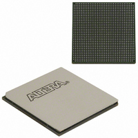
EP3SL150F1152C3N Altera, EP3SL150F1152C3N Datasheet - Page 369

EP3SL150F1152C3N
Manufacturer Part Number
EP3SL150F1152C3N
Description
IC STRATX III FPGA 150K 1152FBGA
Manufacturer
Altera
Series
Stratix® IIIr
Datasheets
1.EP3SL150F780C4N.pdf
(16 pages)
2.EP3SL150F780C4N.pdf
(332 pages)
3.EP3SL150F780C4N.pdf
(456 pages)
Specifications of EP3SL150F1152C3N
Number Of Logic Elements/cells
142500
Number Of Labs/clbs
5700
Total Ram Bits
6390
Number Of I /o
744
Voltage - Supply
0.86 V ~ 1.15 V
Mounting Type
Surface Mount
Operating Temperature
0°C ~ 85°C
Package / Case
1152-FBGA
For Use With
544-2568 - KIT DEVELOPMENT STRATIX III
Lead Free Status / RoHS Status
Lead free / RoHS Compliant
Number Of Gates
-
Other names
544-2408
EP3SL150F1152C3NES
EP3SL150F1152C3NES
Available stocks
Company
Part Number
Manufacturer
Quantity
Price
Company:
Part Number:
EP3SL150F1152C3N
Manufacturer:
ALTERA
Quantity:
490
- Current page: 369 of 456
- Download datasheet (7Mb)
Chapter 11: Configuring Stratix III Devices
JTAG Configuration
JTAG Configuration
© March 2011 Altera Corporation
f
f
1
1
The JTAG has developed a specification for boundary-scan testing. This
boundary-scan test (BST) architecture offers the capability to efficiently test
components on PCBs with tight lead spacing. The BST architecture can test pin
connections without using physical test probes and capture functional data while a
device is operating normally. You can also use the JTAG circuitry to shift
configuration data into the device. The Quartus II software automatically generates
SOFs that can be used for JTAG configuration with a download cable in the Quartus II
software programmer.
For more information about JTAG boundary-scan testing and commands available
using Stratix III devices, refer to the following documents:
■
■
Stratix III devices are designed such that JTAG instructions have precedence over any
device configuration modes. Therefore, JTAG configuration can take place without
waiting for other configuration modes to complete. For example, if you attempt JTAG
configuration of Stratix III devices during PS configuration, PS configuration is
terminated and JTAG configuration begins.
You cannot use the Stratix III decompression or design security features if you are
configuring your Stratix III device when using JTAG-based configuration.
A device operating in JTAG mode uses four required pins, TDI, TDO, TMS, and TCK,
and one optional pin, TRST. The TCK pin has an internal weak pull-down resistor,
while the TDI, TMS, and TRST pins have weak internal pull-up resistors (typically
25 kΩ). JTAG output pin TDO and all JTAG input pins are powered by the
2.5 V/3.0 V/3.3 V V
only LVTTL I/O standard.
All user I/O pins are tri-stated during JTAG configuration.
JTAG pin's function.
The TDO output is powered by the V
recommendations on how to connect a JTAG chain with multiple voltages across the
devices in the chain, refer to the
Devices
IEEE 1149.1 (JTAG) Boundary Scan Testing in Stratix III Device
Stratix III Device Handbook
AN 425: Using the Command-Line Jam STAPL Solution for Device Programming
chapter of the Stratix III Device Handbook.
CCPD
power supply of I/O bank 1A. All the JTAG pins support
IEEE 1149.1 (JTAG) Boundary Scan Testing in Stratix III
CCPD
power supply of I/O bank 1A. For
Stratix III Device Handbook, Volume 1
Table 11–11
chapter of the
explains each
11–37
Related parts for EP3SL150F1152C3N
Image
Part Number
Description
Manufacturer
Datasheet
Request
R

Part Number:
Description:
CYCLONE II STARTER KIT EP2C20N
Manufacturer:
Altera
Datasheet:

Part Number:
Description:
CPLD, EP610 Family, ECMOS Process, 300 Gates, 16 Macro Cells, 16 Reg., 16 User I/Os, 5V Supply, 35 Speed Grade, 24DIP
Manufacturer:
Altera Corporation
Datasheet:

Part Number:
Description:
CPLD, EP610 Family, ECMOS Process, 300 Gates, 16 Macro Cells, 16 Reg., 16 User I/Os, 5V Supply, 15 Speed Grade, 24DIP
Manufacturer:
Altera Corporation
Datasheet:

Part Number:
Description:
Manufacturer:
Altera Corporation
Datasheet:

Part Number:
Description:
CPLD, EP610 Family, ECMOS Process, 300 Gates, 16 Macro Cells, 16 Reg., 16 User I/Os, 5V Supply, 30 Speed Grade, 24DIP
Manufacturer:
Altera Corporation
Datasheet:

Part Number:
Description:
High-performance, low-power erasable programmable logic devices with 8 macrocells, 10ns
Manufacturer:
Altera Corporation
Datasheet:

Part Number:
Description:
High-performance, low-power erasable programmable logic devices with 8 macrocells, 7ns
Manufacturer:
Altera Corporation
Datasheet:

Part Number:
Description:
Classic EPLD
Manufacturer:
Altera Corporation
Datasheet:

Part Number:
Description:
High-performance, low-power erasable programmable logic devices with 8 macrocells, 10ns
Manufacturer:
Altera Corporation
Datasheet:

Part Number:
Description:
Manufacturer:
Altera Corporation
Datasheet:

Part Number:
Description:
Manufacturer:
Altera Corporation
Datasheet:

Part Number:
Description:
Manufacturer:
Altera Corporation
Datasheet:

Part Number:
Description:
CPLD, EP610 Family, ECMOS Process, 300 Gates, 16 Macro Cells, 16 Reg., 16 User I/Os, 5V Supply, 25 Speed Grade, 24DIP
Manufacturer:
Altera Corporation
Datasheet:


