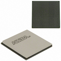
EP3SL150F1152C3N Altera, EP3SL150F1152C3N Datasheet - Page 370

EP3SL150F1152C3N
Manufacturer Part Number
EP3SL150F1152C3N
Description
IC STRATX III FPGA 150K 1152FBGA
Manufacturer
Altera
Series
Stratix® IIIr
Datasheets
1.EP3SL150F780C4N.pdf
(16 pages)
2.EP3SL150F780C4N.pdf
(332 pages)
3.EP3SL150F780C4N.pdf
(456 pages)
Specifications of EP3SL150F1152C3N
Number Of Logic Elements/cells
142500
Number Of Labs/clbs
5700
Total Ram Bits
6390
Number Of I /o
744
Voltage - Supply
0.86 V ~ 1.15 V
Mounting Type
Surface Mount
Operating Temperature
0°C ~ 85°C
Package / Case
1152-FBGA
For Use With
544-2568 - KIT DEVELOPMENT STRATIX III
Lead Free Status / RoHS Status
Lead free / RoHS Compliant
Number Of Gates
-
Other names
544-2408
EP3SL150F1152C3NES
EP3SL150F1152C3NES
Available stocks
Company
Part Number
Manufacturer
Quantity
Price
Company:
Part Number:
EP3SL150F1152C3N
Manufacturer:
ALTERA
Quantity:
490
- Current page: 370 of 456
- Download datasheet (7Mb)
11–38
Table 11–11. Dedicated JTAG Pins
Stratix III Device Handbook, Volume 1
TDI
TDO
TMS
TCK
TRST
Pin Name
Test data input
Test data output
Test mode select
Test clock input
Test reset input
(optional)
1
Pin Type
During JTAG configuration, you can download data to the device on the PCB through
the USB-Blaster, MasterBlaster, ByteBlaster II, ByteBlasterMV, or EthernetBlaster
download cables. Configuring devices through a cable is similar to programming
devices in-system, except you should connect the TRST pin to V
the TAP controller is not reset.
The JRunner™ software driver is developed to configure Altera FPGA devices in
JTAG mode through the ByteBlaster II or ByteBlasterMV download cables for
embedded configurations. For more information, refer to
Software
Driver.
Serial input pin for instructions as well as test and programming data. Data is shifted in
the rising edge of TCK. If the JTAG interface is not required on the board, you can
disable the JTAG circuitry by connecting this pin to V
Serial data output pin for instructions as well as test and programming data. Data is
shifted out on the falling edge of TCK. The pin is tri-stated if data is not being shifted
out of the device. If the JTAG interface is not required on the board, you can disable the
JTAG circuitry by leaving this pin unconnected.
Input pin that provides the control signal to determine the transitions of the TAP
controller state machine. Transitions within the state machine occur on the rising edge
of TCK. Therefore, you must set up TMS before the rising edge of TCK. TMS is
evaluated on the rising edge of TCK. If the JTAG interface is not required on the board,
you can disable the JTAG circuitry by connecting this pin to VCCPD.
The clock input to the BST circuitry. Some operations occur at the rising edge while
others occur at the falling edge. If the JTAG interface is not required on the board, you
can disable the JTAG circuitry by connecting this pin to GND.
Active-low input to asynchronously reset the boundary-scan circuit. The TRST pin is
optional according to IEEE Std. 1149.1. If the JTAG interface is not required on the
board, you can disable the JTAG circuitry by connecting this pin to GND.
Description
Chapter 11: Configuring Stratix III Devices
CC PD
AN 414: The JRunner
.
© March 2011 Altera Corporation
CCPD
. This ensures that
JTAG Configuration
Related parts for EP3SL150F1152C3N
Image
Part Number
Description
Manufacturer
Datasheet
Request
R

Part Number:
Description:
CYCLONE II STARTER KIT EP2C20N
Manufacturer:
Altera
Datasheet:

Part Number:
Description:
CPLD, EP610 Family, ECMOS Process, 300 Gates, 16 Macro Cells, 16 Reg., 16 User I/Os, 5V Supply, 35 Speed Grade, 24DIP
Manufacturer:
Altera Corporation
Datasheet:

Part Number:
Description:
CPLD, EP610 Family, ECMOS Process, 300 Gates, 16 Macro Cells, 16 Reg., 16 User I/Os, 5V Supply, 15 Speed Grade, 24DIP
Manufacturer:
Altera Corporation
Datasheet:

Part Number:
Description:
Manufacturer:
Altera Corporation
Datasheet:

Part Number:
Description:
CPLD, EP610 Family, ECMOS Process, 300 Gates, 16 Macro Cells, 16 Reg., 16 User I/Os, 5V Supply, 30 Speed Grade, 24DIP
Manufacturer:
Altera Corporation
Datasheet:

Part Number:
Description:
High-performance, low-power erasable programmable logic devices with 8 macrocells, 10ns
Manufacturer:
Altera Corporation
Datasheet:

Part Number:
Description:
High-performance, low-power erasable programmable logic devices with 8 macrocells, 7ns
Manufacturer:
Altera Corporation
Datasheet:

Part Number:
Description:
Classic EPLD
Manufacturer:
Altera Corporation
Datasheet:

Part Number:
Description:
High-performance, low-power erasable programmable logic devices with 8 macrocells, 10ns
Manufacturer:
Altera Corporation
Datasheet:

Part Number:
Description:
Manufacturer:
Altera Corporation
Datasheet:

Part Number:
Description:
Manufacturer:
Altera Corporation
Datasheet:

Part Number:
Description:
Manufacturer:
Altera Corporation
Datasheet:

Part Number:
Description:
CPLD, EP610 Family, ECMOS Process, 300 Gates, 16 Macro Cells, 16 Reg., 16 User I/Os, 5V Supply, 25 Speed Grade, 24DIP
Manufacturer:
Altera Corporation
Datasheet:


