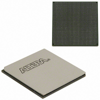
EP3SL150F1152C3N Altera, EP3SL150F1152C3N Datasheet - Page 373

EP3SL150F1152C3N
Manufacturer Part Number
EP3SL150F1152C3N
Description
IC STRATX III FPGA 150K 1152FBGA
Manufacturer
Altera
Series
Stratix® IIIr
Datasheets
1.EP3SL150F780C4N.pdf
(16 pages)
2.EP3SL150F780C4N.pdf
(332 pages)
3.EP3SL150F780C4N.pdf
(456 pages)
Specifications of EP3SL150F1152C3N
Number Of Logic Elements/cells
142500
Number Of Labs/clbs
5700
Total Ram Bits
6390
Number Of I /o
744
Voltage - Supply
0.86 V ~ 1.15 V
Mounting Type
Surface Mount
Operating Temperature
0°C ~ 85°C
Package / Case
1152-FBGA
For Use With
544-2568 - KIT DEVELOPMENT STRATIX III
Lead Free Status / RoHS Status
Lead free / RoHS Compliant
Number Of Gates
-
Other names
544-2408
EP3SL150F1152C3NES
EP3SL150F1152C3NES
Available stocks
Company
Part Number
Manufacturer
Quantity
Price
Company:
Part Number:
EP3SL150F1152C3N
Manufacturer:
ALTERA
Quantity:
490
- Current page: 373 of 456
- Download datasheet (7Mb)
Chapter 11: Configuring Stratix III Devices
JTAG Configuration
Figure 11–20. JTAG Configuration of Multiple Devices Using a Download Cable
Notes to
(1) Connect the pull-up resistor to the same supply voltage as the USB-Blaster, MasterBlaster
(2) Connect the nCONFIG, MSEL[2..0] pins to support a non-JTAG configuration scheme. If you only use JTAG configuration, connect nCONFIG
(3) Pin 6 of the header is a V
(4) You must connect nCE to GND or drive it low for successful JTAG configuration.
(5) Pull-up resistor values can vary from 1 kΩ to 10 kΩ.
© March 2011 Altera Corporation
Pin 1
EthernetBlaster cables. The voltage supply can be connected to the
to V
Serial/USB Communications Cable Data Sheet
no connect.
10-Pin Male Header
Download Cable
(JTAG Mode)
C CPGM
Figure
V CCPD
, and MSEL[2..0] to ground. Pull DCLK either high or low, whichever is convenient on your board.
11–20:
V
(3)
V CCPD (1)
(5)
IO
1 kΩ
V CCPD (1)
You must connect the nCE pin to GND or drive it low during JTAG configuration. In
multi-device FPP, AS, and PS configuration chains, the first device's nCE pin is
connected to GND while its nCEO pin is connected to nCE of the next device in the
chain. The last device's nCE input comes from the previous device, while its nCEO pin
is left floating. In addition, the CONF_DONE and nSTATUS signals are all shared in
multi-device FPP, AS, or PS configuration chains so the devices can enter user mode at
the same time after configuration is complete. When the CONF_DONE and nSTATUS
signals are shared among all the devices, you must configure every device when JTAG
configuration is performed.
If you only use JTAG configuration, Altera recommends that you connect the circuitry
as shown in
isolated, so that each device can enter user mode individually.
After the first device completes configuration in a multi-device configuration chain,
its nCEO pin drives low to activate the second device's nCE pin, which prompts the
second device to begin configuration. Therefore, if these devices are also in a JTAG
chain, make sure the nCE pins are connected to GND during JTAG configuration or
that the devices are JTAG configured in the same order as the configuration chain. As
long as the devices are JTAG configured in the same order as the multi-device
configuration chain, the nCEO of the previous device will drive the nCE of the next
device low when it has successfully been JTAG configured.
(5)
IO
reference voltage for the MasterBlaster output driver. V
V CCPD
(2)
(2)
(2)
V CCPGM (1)
10 kΩ
TDI
nSTATUS
nCONFIG
DCLK
MSEL[2..0]
nCE
TRST
Figure
TMS
Stratix III Device
(4)
for this value. In the USB-Blaster, ByteBlaster II, ByteBlasterMV, and EthernetBlaster, this pin is a
CONF_DONE
TCK
11–20, where each of the CONF_DONE and nSTATUS signals are
TDO
V CCPGM (1)
V CCPD
10 kΩ
(2)
(2)
(2)
V
V CCPGM (1)
CCPD
10 kΩ
TDI
nSTATUS
nCONFIG
DCLK
MSEL[2..0]
nCE
TRST
o
TMS
f the device.
Stratix III Device
(4)
CONF_DONE
IO
TCK
should match the device's V
TDO
(V
V CCPGM (1)
IO
V CCPD
pin), B
10 kΩ
(2)
(2)
(2)
V CCPGM (1)
yteBlaster II, ByteBlasterMV, or
10 kΩ
Stratix III Device Handbook, Volume 1
TDI
nSTATUS
nCONFIG
DCLK
MSEL[2..0]
nCE
TRST
Stratix II or Stratix II GX
TMS
Stratix III Device
(4)
C CP D
Device
CONF_DONE
. Refer to the
TCK
TDO
V CCPGM (1)
MasterBlaster
10 kΩ
11–41
Related parts for EP3SL150F1152C3N
Image
Part Number
Description
Manufacturer
Datasheet
Request
R

Part Number:
Description:
CYCLONE II STARTER KIT EP2C20N
Manufacturer:
Altera
Datasheet:

Part Number:
Description:
CPLD, EP610 Family, ECMOS Process, 300 Gates, 16 Macro Cells, 16 Reg., 16 User I/Os, 5V Supply, 35 Speed Grade, 24DIP
Manufacturer:
Altera Corporation
Datasheet:

Part Number:
Description:
CPLD, EP610 Family, ECMOS Process, 300 Gates, 16 Macro Cells, 16 Reg., 16 User I/Os, 5V Supply, 15 Speed Grade, 24DIP
Manufacturer:
Altera Corporation
Datasheet:

Part Number:
Description:
Manufacturer:
Altera Corporation
Datasheet:

Part Number:
Description:
CPLD, EP610 Family, ECMOS Process, 300 Gates, 16 Macro Cells, 16 Reg., 16 User I/Os, 5V Supply, 30 Speed Grade, 24DIP
Manufacturer:
Altera Corporation
Datasheet:

Part Number:
Description:
High-performance, low-power erasable programmable logic devices with 8 macrocells, 10ns
Manufacturer:
Altera Corporation
Datasheet:

Part Number:
Description:
High-performance, low-power erasable programmable logic devices with 8 macrocells, 7ns
Manufacturer:
Altera Corporation
Datasheet:

Part Number:
Description:
Classic EPLD
Manufacturer:
Altera Corporation
Datasheet:

Part Number:
Description:
High-performance, low-power erasable programmable logic devices with 8 macrocells, 10ns
Manufacturer:
Altera Corporation
Datasheet:

Part Number:
Description:
Manufacturer:
Altera Corporation
Datasheet:

Part Number:
Description:
Manufacturer:
Altera Corporation
Datasheet:

Part Number:
Description:
Manufacturer:
Altera Corporation
Datasheet:

Part Number:
Description:
CPLD, EP610 Family, ECMOS Process, 300 Gates, 16 Macro Cells, 16 Reg., 16 User I/Os, 5V Supply, 25 Speed Grade, 24DIP
Manufacturer:
Altera Corporation
Datasheet:


