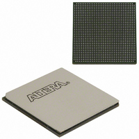
EP3SL150F1152C3N Altera, EP3SL150F1152C3N Datasheet - Page 374

EP3SL150F1152C3N
Manufacturer Part Number
EP3SL150F1152C3N
Description
IC STRATX III FPGA 150K 1152FBGA
Manufacturer
Altera
Series
Stratix® IIIr
Datasheets
1.EP3SL150F780C4N.pdf
(16 pages)
2.EP3SL150F780C4N.pdf
(332 pages)
3.EP3SL150F780C4N.pdf
(456 pages)
Specifications of EP3SL150F1152C3N
Number Of Logic Elements/cells
142500
Number Of Labs/clbs
5700
Total Ram Bits
6390
Number Of I /o
744
Voltage - Supply
0.86 V ~ 1.15 V
Mounting Type
Surface Mount
Operating Temperature
0°C ~ 85°C
Package / Case
1152-FBGA
For Use With
544-2568 - KIT DEVELOPMENT STRATIX III
Lead Free Status / RoHS Status
Lead free / RoHS Compliant
Number Of Gates
-
Other names
544-2408
EP3SL150F1152C3NES
EP3SL150F1152C3NES
Available stocks
Company
Part Number
Manufacturer
Quantity
Price
Company:
Part Number:
EP3SL150F1152C3N
Manufacturer:
ALTERA
Quantity:
490
- Current page: 374 of 456
- Download datasheet (7Mb)
11–42
Stratix III Device Handbook, Volume 1
f
f
1
You can place other Altera devices that have JTAG support in the same JTAG chain for
device programming and configuration.
JTAG configuration support has been enhanced and allows more than 17 Stratix III
devices to be cascaded in a JTAG chain.
For more information about configuring multiple Altera devices in the same
configuration chain, refer to the
Configuration Handbook.
You can configure Stratix III devices using multiple configuration schemes on the
same board. Combining JTAG configuration with passive serial (PS) or active serial
(AS) configuration on your board is useful in the prototyping environment because it
allows multiple methods to configure your FPGA.
For more information about combining JTAG configuration with other configuration
schemes, refer to the
Configuration Handbook.
Figure 11–21
Figure 11–21. JTAG Configuration of a Single Device Using a Microprocessor
Notes to
(1) Connect the pull-up resistor to a supply that provides an acceptable input signal for all devices in the chain. V
(2) Connect the
(3) You must connect nCE to GND or drive it low for successful JTAG configuration.
(4) Microprocessor should use the same I/O standard as V
should be high enough to meet the V
JTAG configuration, connect
whichever is convenient on your board.
Figure
11–21:
nCONFIG
shows JTAG configuration of a Stratix III device with a microprocessor.
Microprocessor
and
ADDR
Combining Different Configuration Schemes
MSEL[2..0]
Memory
nCONFIG
DATA
IH
specification of the I/O on the device.
to V
Configuring Mixed Altera Device Chains
CC PGM
pins to support a non-JTAG configuration scheme. If you use only the
V CCPD
, and
TRST
TRST
TDI
TDI
TCK
TCK
TMS
TMS
TDO
TDO
MSEL[2..0]
Stratix III Device
C CPD
(4)
(4)
(4)
(4)
to drive the JTAG pins.
CONF_DONE
MSEL[2..0]
nSTATUS
nCONFIG
(3) nCE
DCLK
nCEO
to ground. Pull
Chapter 11: Configuring Stratix III Devices
V CCPGM (1)
(2)
(2)
(2)
N.C.
GND
© March 2011 Altera Corporation
10 kΩ
chapter in the
V CCPGM (1)
DCLK
10 kΩ
either high or low,
chapter in the
JTAG Configuration
CCPGM
Related parts for EP3SL150F1152C3N
Image
Part Number
Description
Manufacturer
Datasheet
Request
R

Part Number:
Description:
CYCLONE II STARTER KIT EP2C20N
Manufacturer:
Altera
Datasheet:

Part Number:
Description:
CPLD, EP610 Family, ECMOS Process, 300 Gates, 16 Macro Cells, 16 Reg., 16 User I/Os, 5V Supply, 35 Speed Grade, 24DIP
Manufacturer:
Altera Corporation
Datasheet:

Part Number:
Description:
CPLD, EP610 Family, ECMOS Process, 300 Gates, 16 Macro Cells, 16 Reg., 16 User I/Os, 5V Supply, 15 Speed Grade, 24DIP
Manufacturer:
Altera Corporation
Datasheet:

Part Number:
Description:
Manufacturer:
Altera Corporation
Datasheet:

Part Number:
Description:
CPLD, EP610 Family, ECMOS Process, 300 Gates, 16 Macro Cells, 16 Reg., 16 User I/Os, 5V Supply, 30 Speed Grade, 24DIP
Manufacturer:
Altera Corporation
Datasheet:

Part Number:
Description:
High-performance, low-power erasable programmable logic devices with 8 macrocells, 10ns
Manufacturer:
Altera Corporation
Datasheet:

Part Number:
Description:
High-performance, low-power erasable programmable logic devices with 8 macrocells, 7ns
Manufacturer:
Altera Corporation
Datasheet:

Part Number:
Description:
Classic EPLD
Manufacturer:
Altera Corporation
Datasheet:

Part Number:
Description:
High-performance, low-power erasable programmable logic devices with 8 macrocells, 10ns
Manufacturer:
Altera Corporation
Datasheet:

Part Number:
Description:
Manufacturer:
Altera Corporation
Datasheet:

Part Number:
Description:
Manufacturer:
Altera Corporation
Datasheet:

Part Number:
Description:
Manufacturer:
Altera Corporation
Datasheet:

Part Number:
Description:
CPLD, EP610 Family, ECMOS Process, 300 Gates, 16 Macro Cells, 16 Reg., 16 User I/Os, 5V Supply, 25 Speed Grade, 24DIP
Manufacturer:
Altera Corporation
Datasheet:


