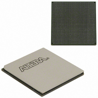
EP3SL150F1152C3N Altera, EP3SL150F1152C3N Datasheet - Page 376

EP3SL150F1152C3N
Manufacturer Part Number
EP3SL150F1152C3N
Description
IC STRATX III FPGA 150K 1152FBGA
Manufacturer
Altera
Series
Stratix® IIIr
Datasheets
1.EP3SL150F780C4N.pdf
(16 pages)
2.EP3SL150F780C4N.pdf
(332 pages)
3.EP3SL150F780C4N.pdf
(456 pages)
Specifications of EP3SL150F1152C3N
Number Of Logic Elements/cells
142500
Number Of Labs/clbs
5700
Total Ram Bits
6390
Number Of I /o
744
Voltage - Supply
0.86 V ~ 1.15 V
Mounting Type
Surface Mount
Operating Temperature
0°C ~ 85°C
Package / Case
1152-FBGA
For Use With
544-2568 - KIT DEVELOPMENT STRATIX III
Lead Free Status / RoHS Status
Lead free / RoHS Compliant
Number Of Gates
-
Other names
544-2408
EP3SL150F1152C3NES
EP3SL150F1152C3NES
Available stocks
Company
Part Number
Manufacturer
Quantity
Price
Company:
Part Number:
EP3SL150F1152C3N
Manufacturer:
ALTERA
Quantity:
490
- Current page: 376 of 456
- Download datasheet (7Mb)
11–44
Table 11–13. Stratix III Configuration Pin Summary
Table 11–14. Dedicated Configuration Pins on the Stratix III Device (Part 1 of 5)
Stratix III Device Handbook, Volume 1
MSEL[2..0]
Notes to
(1) The total number of pins is 30. The total number of dedicated pins is 19.
(2) The JTAG output pin TDO and all JTAG input pins are powered by the 2.5 V/3.0 V/3.3-V V
(3) These dual purpose pins are powered by V
VCCPGM
VCCPD
PORSEL
Pin Name
configuration modes.
Description
Table
11–13:
User Mode
N/A
N/A
N/A
Table 11–14
connected properly on your board for successful configuration. Some of these pins
may not be required for your configuration schemes.
Input/Output
Input
Configuration
describes the dedicated configuration pins, which are required to be
Scheme
CCPGM
All
All
All
during configuration, then are powered by V
(Note 1)
Pin Type
Power
Power
Input
Dedicated
Yes
(Part 2 of 2)
Dedicated power pin. Use this pin to power all dedicated
configuration inputs, dedicated configuration outputs,
dedicated configuration bi-direction pins, and some of
the dual functional pins that are used for configuration.
You must connect this pin to 1.8-V, 2.5-V, 3.0-V, or
3.3-V. V
ms. If V
your Stratix III device will not configure successfully. If
your system does not allow for a VCCPGM ramp-up
time of 100 ms or less, you must hold nCONFIG low
until all power supplies are stable.
Dedicated power pin. Use this pin to power the I/O
pre-drivers, the JTAG input and output pins, and the
design security circuitry.
You must connect this pin to 2.5-V, 3.0-V, or 3.3-V
depending on the I/O standards selected. For 3.3-V I/O
standards, VCCPD=3.3-V, for 3.0-V I/O standards, V
= 3.0 V, for 2.5-V or below I/O standards, V
V
within 100 ms. If V
specified time, your Stratix III device will not configure
successfully. If your system does not allow for a V
ramp-up time of 100 ms or less, you must hold
nCONFIG low until all power supplies are stable.
Dedicated input which selects either a POR time of 12
ms or 100 ms. A logic high (1.8 V, 2.5 V, 3.0 V, 3.3 V)
selects a POR time of approximately 12 ms and a logic
low selects a POR time of approximately 100 ms.
The PORSEL input buffer is powered by VCCPGM and
has an internal 5-kΩ pull-down resistor that is always
active. You should tie the PORSEL pin directly to
VCCPGM or GND.
C CP D
must ramp-up from 0-V to 2.5-V / 3.0-V/3.3-V
C CP GM
C CP GM
CCPD
must ramp-up from 0-V to 3.3-V within 100
is not ramped up within this specified time,
Powered By
CCIO
power supply of I/O bank 1A.
V
C CP GM
while in user mode.This applies for all
CC PD
Chapter 11: Configuring Stratix III Devices
Description
is not ramped up within this
© March 2011 Altera Corporation
Configuration Mode
Device Configuration Pins
All modes
C CP D
= 2.5 V.
C CPD
CC PD
Related parts for EP3SL150F1152C3N
Image
Part Number
Description
Manufacturer
Datasheet
Request
R

Part Number:
Description:
CYCLONE II STARTER KIT EP2C20N
Manufacturer:
Altera
Datasheet:

Part Number:
Description:
CPLD, EP610 Family, ECMOS Process, 300 Gates, 16 Macro Cells, 16 Reg., 16 User I/Os, 5V Supply, 35 Speed Grade, 24DIP
Manufacturer:
Altera Corporation
Datasheet:

Part Number:
Description:
CPLD, EP610 Family, ECMOS Process, 300 Gates, 16 Macro Cells, 16 Reg., 16 User I/Os, 5V Supply, 15 Speed Grade, 24DIP
Manufacturer:
Altera Corporation
Datasheet:

Part Number:
Description:
Manufacturer:
Altera Corporation
Datasheet:

Part Number:
Description:
CPLD, EP610 Family, ECMOS Process, 300 Gates, 16 Macro Cells, 16 Reg., 16 User I/Os, 5V Supply, 30 Speed Grade, 24DIP
Manufacturer:
Altera Corporation
Datasheet:

Part Number:
Description:
High-performance, low-power erasable programmable logic devices with 8 macrocells, 10ns
Manufacturer:
Altera Corporation
Datasheet:

Part Number:
Description:
High-performance, low-power erasable programmable logic devices with 8 macrocells, 7ns
Manufacturer:
Altera Corporation
Datasheet:

Part Number:
Description:
Classic EPLD
Manufacturer:
Altera Corporation
Datasheet:

Part Number:
Description:
High-performance, low-power erasable programmable logic devices with 8 macrocells, 10ns
Manufacturer:
Altera Corporation
Datasheet:

Part Number:
Description:
Manufacturer:
Altera Corporation
Datasheet:

Part Number:
Description:
Manufacturer:
Altera Corporation
Datasheet:

Part Number:
Description:
Manufacturer:
Altera Corporation
Datasheet:

Part Number:
Description:
CPLD, EP610 Family, ECMOS Process, 300 Gates, 16 Macro Cells, 16 Reg., 16 User I/Os, 5V Supply, 25 Speed Grade, 24DIP
Manufacturer:
Altera Corporation
Datasheet:


