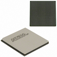
EP3SL150F1152C3N Altera, EP3SL150F1152C3N Datasheet - Page 412

EP3SL150F1152C3N
Manufacturer Part Number
EP3SL150F1152C3N
Description
IC STRATX III FPGA 150K 1152FBGA
Manufacturer
Altera
Series
Stratix® IIIr
Datasheets
1.EP3SL150F780C4N.pdf
(16 pages)
2.EP3SL150F780C4N.pdf
(332 pages)
3.EP3SL150F780C4N.pdf
(456 pages)
Specifications of EP3SL150F1152C3N
Number Of Logic Elements/cells
142500
Number Of Labs/clbs
5700
Total Ram Bits
6390
Number Of I /o
744
Voltage - Supply
0.86 V ~ 1.15 V
Mounting Type
Surface Mount
Operating Temperature
0°C ~ 85°C
Package / Case
1152-FBGA
For Use With
544-2568 - KIT DEVELOPMENT STRATIX III
Lead Free Status / RoHS Status
Lead free / RoHS Compliant
Number Of Gates
-
Other names
544-2408
EP3SL150F1152C3NES
EP3SL150F1152C3NES
Available stocks
Company
Part Number
Manufacturer
Quantity
Price
Company:
Part Number:
EP3SL150F1152C3N
Manufacturer:
ALTERA
Quantity:
490
- Current page: 412 of 456
- Download datasheet (7Mb)
13–14
Figure 13–11. EXTEST Shift Data Register Waveforms
Note to
(1) Data stored in the boundary-scan register is shifted out of TDO.
(2) After boundary-scan register data has been shifted out, data entered into TDI will shift out of TDO.
Stratix III Device Handbook, Volume 1
Figure
TAP_STATE
TMS
TDO
TCK
TDI
13–11:
SHIFT_IR
EXTEST mode selects data differently than SAMPLE/PRELOAD mode. EXTEST chooses
data from the update registers as the source of the output and output-enable signals.
After the EXTEST instruction code is entered, the multiplexers select the update
register data. Therefore, data stored in these registers from a previous EXTEST or
SAMPLE/PRELOAD test cycle can be forced onto the pin signals. In the capture phase,
the results of this test data are stored in the capture registers and then shifted out of
TDO during the shift phase. You can then store new test data in the update registers
during the update phase.
The EXTEST waveform diagram in
waveform diagram, except for the instruction code. The data shifted out of TDO
consists of the data that was present in the capture registers after the capture phase.
New test data shifted into the TDI pin appears at the TDO pin after being clocked
through the entire boundary-scan register.
Instruction Code
EXIT1_IR
UPDATE_IR
SELECT_DR
CAPTURE_DR
Chapter 13: IEEE 1149.1 (JTAG) Boundary-Scan Testing in Stratix III Devices
Figure 13–11
(1)
resembles the SAMPLE/PRELOAD
IEEE Std. 1149.1 BST Operation Control
SHIFT_DR
© July 2010 Altera Corporation
(2)
EXIT1_DR
UPDATE_DR
Related parts for EP3SL150F1152C3N
Image
Part Number
Description
Manufacturer
Datasheet
Request
R

Part Number:
Description:
CYCLONE II STARTER KIT EP2C20N
Manufacturer:
Altera
Datasheet:

Part Number:
Description:
CPLD, EP610 Family, ECMOS Process, 300 Gates, 16 Macro Cells, 16 Reg., 16 User I/Os, 5V Supply, 35 Speed Grade, 24DIP
Manufacturer:
Altera Corporation
Datasheet:

Part Number:
Description:
CPLD, EP610 Family, ECMOS Process, 300 Gates, 16 Macro Cells, 16 Reg., 16 User I/Os, 5V Supply, 15 Speed Grade, 24DIP
Manufacturer:
Altera Corporation
Datasheet:

Part Number:
Description:
Manufacturer:
Altera Corporation
Datasheet:

Part Number:
Description:
CPLD, EP610 Family, ECMOS Process, 300 Gates, 16 Macro Cells, 16 Reg., 16 User I/Os, 5V Supply, 30 Speed Grade, 24DIP
Manufacturer:
Altera Corporation
Datasheet:

Part Number:
Description:
High-performance, low-power erasable programmable logic devices with 8 macrocells, 10ns
Manufacturer:
Altera Corporation
Datasheet:

Part Number:
Description:
High-performance, low-power erasable programmable logic devices with 8 macrocells, 7ns
Manufacturer:
Altera Corporation
Datasheet:

Part Number:
Description:
Classic EPLD
Manufacturer:
Altera Corporation
Datasheet:

Part Number:
Description:
High-performance, low-power erasable programmable logic devices with 8 macrocells, 10ns
Manufacturer:
Altera Corporation
Datasheet:

Part Number:
Description:
Manufacturer:
Altera Corporation
Datasheet:

Part Number:
Description:
Manufacturer:
Altera Corporation
Datasheet:

Part Number:
Description:
Manufacturer:
Altera Corporation
Datasheet:

Part Number:
Description:
CPLD, EP610 Family, ECMOS Process, 300 Gates, 16 Macro Cells, 16 Reg., 16 User I/Os, 5V Supply, 25 Speed Grade, 24DIP
Manufacturer:
Altera Corporation
Datasheet:


