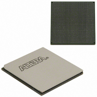
EP3SL150F1152C3N Altera, EP3SL150F1152C3N Datasheet - Page 48

EP3SL150F1152C3N
Manufacturer Part Number
EP3SL150F1152C3N
Description
IC STRATX III FPGA 150K 1152FBGA
Manufacturer
Altera
Series
Stratix® IIIr
Datasheets
1.EP3SL150F780C4N.pdf
(16 pages)
2.EP3SL150F780C4N.pdf
(332 pages)
3.EP3SL150F780C4N.pdf
(456 pages)
Specifications of EP3SL150F1152C3N
Number Of Logic Elements/cells
142500
Number Of Labs/clbs
5700
Total Ram Bits
6390
Number Of I /o
744
Voltage - Supply
0.86 V ~ 1.15 V
Mounting Type
Surface Mount
Operating Temperature
0°C ~ 85°C
Package / Case
1152-FBGA
For Use With
544-2568 - KIT DEVELOPMENT STRATIX III
Lead Free Status / RoHS Status
Lead free / RoHS Compliant
Number Of Gates
-
Other names
544-2408
EP3SL150F1152C3NES
EP3SL150F1152C3NES
Available stocks
Company
Part Number
Manufacturer
Quantity
Price
Company:
Part Number:
EP3SL150F1152C3N
Manufacturer:
ALTERA
Quantity:
490
- Current page: 48 of 456
- Download datasheet (7Mb)
2–4
Figure 2–3. Direct Link Connection
LAB Control Signals
Stratix III Device Handbook, Volume 1
Direct link
interconnect
to left
block, DSP block, or IOE output
ALMs
Direct link interconnect from
left LAB, TriMatrix memory
Figure
Each LAB contains dedicated logic for driving control signals to its ALMs. The control
signals include three clocks, three clock enables, two asynchronous clears, a
synchronous clear, and synchronous load control signals. This gives a maximum of 10
control signals at a time. Although you generally use synchronous load and clear
signals when implementing counters, you can also use them with other functions.
Each LAB has two unique clock sources and three clock enable signals, as shown in
Figure
sources and three clock enable signals. Each LAB's clock and clock enable signals are
linked. For example, any ALM in a particular LAB using the labclk1 signal also uses
labclkena1 signal. If the LAB uses both the rising and falling edges of a clock, it also
uses two LAB-wide clock signals. De-asserting the clock enable signal turns off the
corresponding LAB-wide clock.
The LAB row clocks [5..0] and LAB local interconnect generate the LAB-wide control
signals. The MultiTrack
signal distribution in addition to data.
generation circuit.
2–3shows the direct link connection.
2–4. The LAB control block can generate up to three clocks using the two clock
MLAB
Interconnect
Local
TM
Chapter 2: Logic Array Blocks and Adaptive Logic Modules in Stratix III Devices
interconnect's inherent low skew allows clock and control
Figure
LAB
2–4shows the LAB control signal
ALMs
Direct link
interconnect
to right
Direct link interconnect from
right LAB, TriMatrix memory
block, DSP block, or IOE output
© February 2009 Altera Corporation
Logic Array Blocks
Related parts for EP3SL150F1152C3N
Image
Part Number
Description
Manufacturer
Datasheet
Request
R

Part Number:
Description:
CYCLONE II STARTER KIT EP2C20N
Manufacturer:
Altera
Datasheet:

Part Number:
Description:
CPLD, EP610 Family, ECMOS Process, 300 Gates, 16 Macro Cells, 16 Reg., 16 User I/Os, 5V Supply, 35 Speed Grade, 24DIP
Manufacturer:
Altera Corporation
Datasheet:

Part Number:
Description:
CPLD, EP610 Family, ECMOS Process, 300 Gates, 16 Macro Cells, 16 Reg., 16 User I/Os, 5V Supply, 15 Speed Grade, 24DIP
Manufacturer:
Altera Corporation
Datasheet:

Part Number:
Description:
Manufacturer:
Altera Corporation
Datasheet:

Part Number:
Description:
CPLD, EP610 Family, ECMOS Process, 300 Gates, 16 Macro Cells, 16 Reg., 16 User I/Os, 5V Supply, 30 Speed Grade, 24DIP
Manufacturer:
Altera Corporation
Datasheet:

Part Number:
Description:
High-performance, low-power erasable programmable logic devices with 8 macrocells, 10ns
Manufacturer:
Altera Corporation
Datasheet:

Part Number:
Description:
High-performance, low-power erasable programmable logic devices with 8 macrocells, 7ns
Manufacturer:
Altera Corporation
Datasheet:

Part Number:
Description:
Classic EPLD
Manufacturer:
Altera Corporation
Datasheet:

Part Number:
Description:
High-performance, low-power erasable programmable logic devices with 8 macrocells, 10ns
Manufacturer:
Altera Corporation
Datasheet:

Part Number:
Description:
Manufacturer:
Altera Corporation
Datasheet:

Part Number:
Description:
Manufacturer:
Altera Corporation
Datasheet:

Part Number:
Description:
Manufacturer:
Altera Corporation
Datasheet:

Part Number:
Description:
CPLD, EP610 Family, ECMOS Process, 300 Gates, 16 Macro Cells, 16 Reg., 16 User I/Os, 5V Supply, 25 Speed Grade, 24DIP
Manufacturer:
Altera Corporation
Datasheet:


