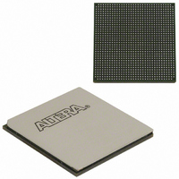
EP3SL150F1152C3N Altera, EP3SL150F1152C3N Datasheet - Page 65

EP3SL150F1152C3N
Manufacturer Part Number
EP3SL150F1152C3N
Description
IC STRATX III FPGA 150K 1152FBGA
Manufacturer
Altera
Series
Stratix® IIIr
Datasheets
1.EP3SL150F780C4N.pdf
(16 pages)
2.EP3SL150F780C4N.pdf
(332 pages)
3.EP3SL150F780C4N.pdf
(456 pages)
Specifications of EP3SL150F1152C3N
Number Of Logic Elements/cells
142500
Number Of Labs/clbs
5700
Total Ram Bits
6390
Number Of I /o
744
Voltage - Supply
0.86 V ~ 1.15 V
Mounting Type
Surface Mount
Operating Temperature
0°C ~ 85°C
Package / Case
1152-FBGA
For Use With
544-2568 - KIT DEVELOPMENT STRATIX III
Lead Free Status / RoHS Status
Lead free / RoHS Compliant
Number Of Gates
-
Other names
544-2408
EP3SL150F1152C3NES
EP3SL150F1152C3NES
Available stocks
Company
Part Number
Manufacturer
Quantity
Price
Company:
Part Number:
EP3SL150F1152C3N
Manufacturer:
ALTERA
Quantity:
490
- Current page: 65 of 456
- Download datasheet (7Mb)
Chapter 2: Logic Array Blocks and Adaptive Logic Modules in Stratix III Devices
Conclusion
LAB Power Management Techniques
Conclusion
Chapter Revision History
Table 2–1. Chapter Revision History(Sheet 1 of 2)
© February 2009 Altera Corporation
February 2009,
version 1.5
October 2008,
version 1.4
Date and Revision
f
f
Removed “Referenced Documents” section.
■
■
The following techniques are used to manage static and dynamic power consumption
within the LAB:
■
■
■
■
Refer to the
details on implementation.
For detailed information about Stratix III programmable power capabilities, refer to
the
volume 1 of the Stratix III Device Handbook.
Logic array block and adaptive logic modules are the basic building blocks of the
Stratix III device. You can use these to configure logic functions, arithmetic functions,
and register functions. The ALM provides advanced features with efficient logic
utilization and is completely backward-compatible.
Table
Updated “LAB Control Signals”, and “Carry Chain” Sections.
Updated New Document Format.
Stratix III low-voltage devices (L ordering code suffix) offer selectable core voltage
to reduce both DC and AC power.
To save AC power, Quartus II forces all adder inputs low when ALM adders are
not in use.
Stratix III LABs operate in high-performance mode or low-power mode. The
Quartus II software automatically chooses the appropriate mode for an LAB based
on the design to optimize speed vs. leakage trade-offs.
Clocks represent a significant portion of dynamic power consumption due to their
high switching activity and long paths. The LAB clock that distributes a clock
signal to registers within a LAB is a significant contributor to overall clock power
consumption. Each LAB's clock and clock enable signal are linked. For example, a
combinational ALUT or register in a particular LAB using the labclk1 signal also
uses the labclkena1 signal. To disable LAB-wide clock power consumption
without disabling the entire clock tree, use the LAB-wide clock enable to gate the
LAB-wide clock. The Quartus II software automatically promotes register-level
clock enable signals to the LAB-level. All registers within an LAB that share a
common clock and clock enable are controlled by a shared gated clock. To take
advantage of these clock enables, use a clock enable construct in your HDL code
for the registered logic.
Programmable Power and Temperature Sensing Diode in Stratix III Devices
2–1shows the revision history for this document.
Power Optimization
Changes Made
chapter in section 3 of the Quartus II Handbook for
Stratix III Device Handbook, Volume 1
Summary of Changes
—
—
chapter in
2–21
Related parts for EP3SL150F1152C3N
Image
Part Number
Description
Manufacturer
Datasheet
Request
R

Part Number:
Description:
CYCLONE II STARTER KIT EP2C20N
Manufacturer:
Altera
Datasheet:

Part Number:
Description:
CPLD, EP610 Family, ECMOS Process, 300 Gates, 16 Macro Cells, 16 Reg., 16 User I/Os, 5V Supply, 35 Speed Grade, 24DIP
Manufacturer:
Altera Corporation
Datasheet:

Part Number:
Description:
CPLD, EP610 Family, ECMOS Process, 300 Gates, 16 Macro Cells, 16 Reg., 16 User I/Os, 5V Supply, 15 Speed Grade, 24DIP
Manufacturer:
Altera Corporation
Datasheet:

Part Number:
Description:
Manufacturer:
Altera Corporation
Datasheet:

Part Number:
Description:
CPLD, EP610 Family, ECMOS Process, 300 Gates, 16 Macro Cells, 16 Reg., 16 User I/Os, 5V Supply, 30 Speed Grade, 24DIP
Manufacturer:
Altera Corporation
Datasheet:

Part Number:
Description:
High-performance, low-power erasable programmable logic devices with 8 macrocells, 10ns
Manufacturer:
Altera Corporation
Datasheet:

Part Number:
Description:
High-performance, low-power erasable programmable logic devices with 8 macrocells, 7ns
Manufacturer:
Altera Corporation
Datasheet:

Part Number:
Description:
Classic EPLD
Manufacturer:
Altera Corporation
Datasheet:

Part Number:
Description:
High-performance, low-power erasable programmable logic devices with 8 macrocells, 10ns
Manufacturer:
Altera Corporation
Datasheet:

Part Number:
Description:
Manufacturer:
Altera Corporation
Datasheet:

Part Number:
Description:
Manufacturer:
Altera Corporation
Datasheet:

Part Number:
Description:
Manufacturer:
Altera Corporation
Datasheet:

Part Number:
Description:
CPLD, EP610 Family, ECMOS Process, 300 Gates, 16 Macro Cells, 16 Reg., 16 User I/Os, 5V Supply, 25 Speed Grade, 24DIP
Manufacturer:
Altera Corporation
Datasheet:


