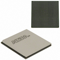
EP3SL150F1152C3N Altera, EP3SL150F1152C3N Datasheet - Page 75

EP3SL150F1152C3N
Manufacturer Part Number
EP3SL150F1152C3N
Description
IC STRATX III FPGA 150K 1152FBGA
Manufacturer
Altera
Series
Stratix® IIIr
Datasheets
1.EP3SL150F780C4N.pdf
(16 pages)
2.EP3SL150F780C4N.pdf
(332 pages)
3.EP3SL150F780C4N.pdf
(456 pages)
Specifications of EP3SL150F1152C3N
Number Of Logic Elements/cells
142500
Number Of Labs/clbs
5700
Total Ram Bits
6390
Number Of I /o
744
Voltage - Supply
0.86 V ~ 1.15 V
Mounting Type
Surface Mount
Operating Temperature
0°C ~ 85°C
Package / Case
1152-FBGA
For Use With
544-2568 - KIT DEVELOPMENT STRATIX III
Lead Free Status / RoHS Status
Lead free / RoHS Compliant
Number Of Gates
-
Other names
544-2408
EP3SL150F1152C3NES
EP3SL150F1152C3NES
Available stocks
Company
Part Number
Manufacturer
Quantity
Price
Company:
Part Number:
EP3SL150F1152C3N
Manufacturer:
ALTERA
Quantity:
490
- Current page: 75 of 456
- Download datasheet (7Mb)
Chapter 3: MultiTrack Interconnect in Stratix III Devices
DSP Block Interface
Figure 3–6. M144K Row Unit Interface to Interconnect
DSP Block Interface
© October 2008 Altera Corporation
Direct Link
Interconnects
LAB
C4 Interconnects
Stratix III device DSP block input registers can generate a shift register that cascades
down in the same DSP block column. Dedicated connections between DSP blocks
provide fast connections between the shift register inputs to cascade the shift register
chains. You can cascade registers within multiple DSP blocks for 9-bit or 18-bit finite
impulse response (FIR) filters larger than four taps, with additional adder stages
implemented in ALMs. If the DSP block is configured as 36-bit blocks, the adder,
subtractor, or accumulator stages are implemented in ALMs. Each DSP block can
route the shift register chain out of the block to cascade multiple columns of DSP
blocks.
The DSP block is divided into four block units that interface with four LAB rows on
the left and right. You can consider each block unit as two 18-bit multipliers followed
by an adder with 72 inputs and 36 outputs. A local interconnect region is associated
with each DSP block. Like a LAB, this interconnect region can be fed with 20 direct
link interconnects from the LAB to the left or right of the DSP block in the same row.
R4 and C4 routing resources can access the DSP block's local interconnect region.
These outputs work similarly to LAB outputs. Eighteen outputs from the DSP block
can drive to the left LAB through direct link interconnects and eighteen can drive to
the right LAB though direct link interconnects. All 36 outputs can drive to R4 and C4
routing interconnects. Outputs can drive right- or left-column routing.
Figure 3–8
M144K Block to
LAB Row Interface
Block Interconnect Region
20
Row Interface Block
show the DSP block interfaces to LAB rows.
Up to 14
Up to 5
M144K Block
datain_a[ ]
addressa[ ]
addressstall
rden/wren
byteena[ ]
clocken_a
clock_a
aclr
dataout_a[ ]
R4 Interconnects
Row Interface Block
Up to 16
Up to 10
Stratix III Device Handbook, Volume 1
M144K Block to
LAB Row Interface
Block Interconnect Region
20
C4 Interconnects
Figure 3–7
LAB
and
3–9
Direct Link
Interconnects
Related parts for EP3SL150F1152C3N
Image
Part Number
Description
Manufacturer
Datasheet
Request
R

Part Number:
Description:
CYCLONE II STARTER KIT EP2C20N
Manufacturer:
Altera
Datasheet:

Part Number:
Description:
CPLD, EP610 Family, ECMOS Process, 300 Gates, 16 Macro Cells, 16 Reg., 16 User I/Os, 5V Supply, 35 Speed Grade, 24DIP
Manufacturer:
Altera Corporation
Datasheet:

Part Number:
Description:
CPLD, EP610 Family, ECMOS Process, 300 Gates, 16 Macro Cells, 16 Reg., 16 User I/Os, 5V Supply, 15 Speed Grade, 24DIP
Manufacturer:
Altera Corporation
Datasheet:

Part Number:
Description:
Manufacturer:
Altera Corporation
Datasheet:

Part Number:
Description:
CPLD, EP610 Family, ECMOS Process, 300 Gates, 16 Macro Cells, 16 Reg., 16 User I/Os, 5V Supply, 30 Speed Grade, 24DIP
Manufacturer:
Altera Corporation
Datasheet:

Part Number:
Description:
High-performance, low-power erasable programmable logic devices with 8 macrocells, 10ns
Manufacturer:
Altera Corporation
Datasheet:

Part Number:
Description:
High-performance, low-power erasable programmable logic devices with 8 macrocells, 7ns
Manufacturer:
Altera Corporation
Datasheet:

Part Number:
Description:
Classic EPLD
Manufacturer:
Altera Corporation
Datasheet:

Part Number:
Description:
High-performance, low-power erasable programmable logic devices with 8 macrocells, 10ns
Manufacturer:
Altera Corporation
Datasheet:

Part Number:
Description:
Manufacturer:
Altera Corporation
Datasheet:

Part Number:
Description:
Manufacturer:
Altera Corporation
Datasheet:

Part Number:
Description:
Manufacturer:
Altera Corporation
Datasheet:

Part Number:
Description:
CPLD, EP610 Family, ECMOS Process, 300 Gates, 16 Macro Cells, 16 Reg., 16 User I/Os, 5V Supply, 25 Speed Grade, 24DIP
Manufacturer:
Altera Corporation
Datasheet:


