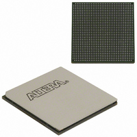
EP3SL150F1152C3N Altera, EP3SL150F1152C3N Datasheet - Page 85

EP3SL150F1152C3N
Manufacturer Part Number
EP3SL150F1152C3N
Description
IC STRATX III FPGA 150K 1152FBGA
Manufacturer
Altera
Series
Stratix® IIIr
Datasheets
1.EP3SL150F780C4N.pdf
(16 pages)
2.EP3SL150F780C4N.pdf
(332 pages)
3.EP3SL150F780C4N.pdf
(456 pages)
Specifications of EP3SL150F1152C3N
Number Of Logic Elements/cells
142500
Number Of Labs/clbs
5700
Total Ram Bits
6390
Number Of I /o
744
Voltage - Supply
0.86 V ~ 1.15 V
Mounting Type
Surface Mount
Operating Temperature
0°C ~ 85°C
Package / Case
1152-FBGA
For Use With
544-2568 - KIT DEVELOPMENT STRATIX III
Lead Free Status / RoHS Status
Lead free / RoHS Compliant
Number Of Gates
-
Other names
544-2408
EP3SL150F1152C3NES
EP3SL150F1152C3NES
Available stocks
Company
Part Number
Manufacturer
Quantity
Price
Company:
Part Number:
EP3SL150F1152C3N
Manufacturer:
ALTERA
Quantity:
490
- Current page: 85 of 456
- Download datasheet (7Mb)
Chapter 4: TriMatrix Embedded Memory Blocks in Stratix III Devices
Overview
Figure 4–2. Stratix III Byte-Enable Functional Waveform for MLABs
Packed Mode Support
Address Clock Enable Support
© May 2009 Altera Corporation
current data: q (asynch)
contents at a1
contents at a0
contents at a2
address
byteena
inclock
wren
data
Figure 4–2
control the operations of the MLABs. The write operation in MLABs is triggered by
failing clock edges.
Stratix III M9K and M144K blocks support packed mode. The packed mode feature
packs two independent single-port RAMs into one memory block. The Quartus II
software automatically implements packed mode where appropriate by placing the
physical RAM block into true dual-port mode and using the MSB of the address to
distinguish between the two logical RAMs. The size of each independent single-port
RAM must not exceed half of the target block size.
All Stratix III memory blocks support address clock enable, which holds the previous
address value for as long as the signal is enabled (addressstall = 1). When the
memory blocks are configured in dual-port mode, each port has its own independent
address clock enable. The default value for the address clock enable signals is low
(disabled).
XXXX
an
XX
doutn
FFFF
FFFF
shows how the write enable (wren) and byte-enable (byteena) signals
FFFF
a0
10
FFFF
ABFF
ABCD
FFFF
a1
01
FFCD
FFFF
a2
11
ABFF
ABCD
a0
ABFF
FFCD
Stratix III Device Handbook, Volume 1
ABCD
a1
XXXX
XX
FFCD
a2
FFCD
4–5
Related parts for EP3SL150F1152C3N
Image
Part Number
Description
Manufacturer
Datasheet
Request
R

Part Number:
Description:
CYCLONE II STARTER KIT EP2C20N
Manufacturer:
Altera
Datasheet:

Part Number:
Description:
CPLD, EP610 Family, ECMOS Process, 300 Gates, 16 Macro Cells, 16 Reg., 16 User I/Os, 5V Supply, 35 Speed Grade, 24DIP
Manufacturer:
Altera Corporation
Datasheet:

Part Number:
Description:
CPLD, EP610 Family, ECMOS Process, 300 Gates, 16 Macro Cells, 16 Reg., 16 User I/Os, 5V Supply, 15 Speed Grade, 24DIP
Manufacturer:
Altera Corporation
Datasheet:

Part Number:
Description:
Manufacturer:
Altera Corporation
Datasheet:

Part Number:
Description:
CPLD, EP610 Family, ECMOS Process, 300 Gates, 16 Macro Cells, 16 Reg., 16 User I/Os, 5V Supply, 30 Speed Grade, 24DIP
Manufacturer:
Altera Corporation
Datasheet:

Part Number:
Description:
High-performance, low-power erasable programmable logic devices with 8 macrocells, 10ns
Manufacturer:
Altera Corporation
Datasheet:

Part Number:
Description:
High-performance, low-power erasable programmable logic devices with 8 macrocells, 7ns
Manufacturer:
Altera Corporation
Datasheet:

Part Number:
Description:
Classic EPLD
Manufacturer:
Altera Corporation
Datasheet:

Part Number:
Description:
High-performance, low-power erasable programmable logic devices with 8 macrocells, 10ns
Manufacturer:
Altera Corporation
Datasheet:

Part Number:
Description:
Manufacturer:
Altera Corporation
Datasheet:

Part Number:
Description:
Manufacturer:
Altera Corporation
Datasheet:

Part Number:
Description:
Manufacturer:
Altera Corporation
Datasheet:

Part Number:
Description:
CPLD, EP610 Family, ECMOS Process, 300 Gates, 16 Macro Cells, 16 Reg., 16 User I/Os, 5V Supply, 25 Speed Grade, 24DIP
Manufacturer:
Altera Corporation
Datasheet:


