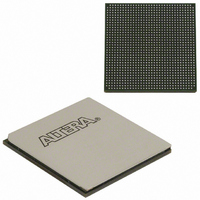
EP3SL150F1152C3N Altera, EP3SL150F1152C3N Datasheet - Page 94

EP3SL150F1152C3N
Manufacturer Part Number
EP3SL150F1152C3N
Description
IC STRATX III FPGA 150K 1152FBGA
Manufacturer
Altera
Series
Stratix® IIIr
Datasheets
1.EP3SL150F780C4N.pdf
(16 pages)
2.EP3SL150F780C4N.pdf
(332 pages)
3.EP3SL150F780C4N.pdf
(456 pages)
Specifications of EP3SL150F1152C3N
Number Of Logic Elements/cells
142500
Number Of Labs/clbs
5700
Total Ram Bits
6390
Number Of I /o
744
Voltage - Supply
0.86 V ~ 1.15 V
Mounting Type
Surface Mount
Operating Temperature
0°C ~ 85°C
Package / Case
1152-FBGA
For Use With
544-2568 - KIT DEVELOPMENT STRATIX III
Lead Free Status / RoHS Status
Lead free / RoHS Compliant
Number Of Gates
-
Other names
544-2408
EP3SL150F1152C3NES
EP3SL150F1152C3NES
Available stocks
Company
Part Number
Manufacturer
Quantity
Price
Company:
Part Number:
EP3SL150F1152C3N
Manufacturer:
ALTERA
Quantity:
490
- Current page: 94 of 456
- Download datasheet (7Mb)
4–14
Figure 4–13. Stratix III Simple Dual-Port Timing Waveforms for M9K and M144K
Figure 4–14. Stratix III Simple Dual-Port Timing Waveforms for MLABs
Stratix III Device Handbook, Volume 1
q (asynch)
wraddress
q (asynch)
rdaddress
wraddress
rdaddress
wrclock
wrclock
rdclock
rdclock
wren
data
rden
wren
data
rden
doutn-1
din-1
doutn-1
din-1
an-1
an-1
In simple dual-port mode, M9K and M144K blocks support separate write-enable and
read-enable signals. You can save power by keeping the read-enable signal low
(inactive) when not reading. Read-during-write operations to the same address can
either output a don’t care value or old data. To choose the desired behavior, set the
read-during-write behavior to either don’t care or old data in the RAM MegaWizard
Plug-In Manager in the Quartus II software. See
for more details about this behavior.
MLABs only support a write-enable signal. Read-during-write behavior for the
MLABs can be either don’t care, new data, or old data. The available choices depend
on the configuration of the MLAB.
Figure 4–13
dual-port mode with unregistered outputs in M9K and M144K. Registering the
RAM’s outputs would simply delay the q output by one clock cycle in M9k and
M144K.
Figure 4–14
dual-port mode with unregistered outputs in MLABs. In MLABs, the write operation
is triggered by the falling clock edges.
bn
bn
an
an
din
din
shows the timing waveforms for read and write operations in simple
shows the timing waveforms for read and write operations in simple
doutn
doutn
b0
a0
b0
a0
a1
a1
Chapter 4: TriMatrix Embedded Memory Blocks in Stratix III Devices
dout0
dout0
a2
b1
b1
a2
a3
a3
“Read During Write” on page 4–21
din4
b2
din4
b2
a4
a4
© May 2009 Altera Corporation
din5
din5
a5
a5
b3
b3
a6
a6
din6
din6
Overview
Related parts for EP3SL150F1152C3N
Image
Part Number
Description
Manufacturer
Datasheet
Request
R

Part Number:
Description:
CYCLONE II STARTER KIT EP2C20N
Manufacturer:
Altera
Datasheet:

Part Number:
Description:
CPLD, EP610 Family, ECMOS Process, 300 Gates, 16 Macro Cells, 16 Reg., 16 User I/Os, 5V Supply, 35 Speed Grade, 24DIP
Manufacturer:
Altera Corporation
Datasheet:

Part Number:
Description:
CPLD, EP610 Family, ECMOS Process, 300 Gates, 16 Macro Cells, 16 Reg., 16 User I/Os, 5V Supply, 15 Speed Grade, 24DIP
Manufacturer:
Altera Corporation
Datasheet:

Part Number:
Description:
Manufacturer:
Altera Corporation
Datasheet:

Part Number:
Description:
CPLD, EP610 Family, ECMOS Process, 300 Gates, 16 Macro Cells, 16 Reg., 16 User I/Os, 5V Supply, 30 Speed Grade, 24DIP
Manufacturer:
Altera Corporation
Datasheet:

Part Number:
Description:
High-performance, low-power erasable programmable logic devices with 8 macrocells, 10ns
Manufacturer:
Altera Corporation
Datasheet:

Part Number:
Description:
High-performance, low-power erasable programmable logic devices with 8 macrocells, 7ns
Manufacturer:
Altera Corporation
Datasheet:

Part Number:
Description:
Classic EPLD
Manufacturer:
Altera Corporation
Datasheet:

Part Number:
Description:
High-performance, low-power erasable programmable logic devices with 8 macrocells, 10ns
Manufacturer:
Altera Corporation
Datasheet:

Part Number:
Description:
Manufacturer:
Altera Corporation
Datasheet:

Part Number:
Description:
Manufacturer:
Altera Corporation
Datasheet:

Part Number:
Description:
Manufacturer:
Altera Corporation
Datasheet:

Part Number:
Description:
CPLD, EP610 Family, ECMOS Process, 300 Gates, 16 Macro Cells, 16 Reg., 16 User I/Os, 5V Supply, 25 Speed Grade, 24DIP
Manufacturer:
Altera Corporation
Datasheet:


