MM908E626AVEK Freescale Semiconductor, MM908E626AVEK Datasheet - Page 15
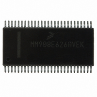
MM908E626AVEK
Manufacturer Part Number
MM908E626AVEK
Description
IC STEPPER MOTOR DRIVER 54-SOIC
Manufacturer
Freescale Semiconductor
Type
Stepper Motor Driverr
Datasheet
1.MM908E626AVEK.pdf
(44 pages)
Specifications of MM908E626AVEK
Applications
Automotive Mirror Control
Core Processor
HC08
Program Memory Type
FLASH (16 kB)
Controller Series
908E
Ram Size
512 x 8
Interface
SCI, SPI
Number Of I /o
13
Voltage - Supply
8 V ~ 18 V
Operating Temperature
-40°C ~ 115°C
Mounting Type
Surface Mount
Package / Case
54-SOIC (7.5mm Width) Exposed Pad, 54-eSOIC, 54-HSOIC
Product
Stepper Motor Controllers / Drivers
Supply Current
20 mA
Lead Free Status / RoHS Status
Lead free / RoHS Compliant
Available stocks
Company
Part Number
Manufacturer
Quantity
Price

Part Number:
MM908E626AVEK
Manufacturer:
FREESCALE
Quantity:
20 000


CURRENT LIMITATION FREQUENCY INPUT PIN
(FGEN)
frequency. This input is not a real PWM input pin; it should
just supply the period of the PWM. The duty cycle will be
generated automatically.
be in the range of 0.1kHz to 20kHz.
BACK ELECTROMAGNETIC FORCE OUTPUT PIN
(BEMF)
electromagnetic force (BEMF). This feature allows stall
detection and coil failures in step motor applications. In order
to evaluate this signal the pin must be directly connected to
pin PTD0 / TACH0 / BEMF.
RESET PIN (
an open drain with pull-up resistor and must be connected to
the
INTERRUPT PIN (
indicating errors or wake-up events. It is an open drain with
pull-up resistor and must be connected to the
MCU.
SLAVE SELECT PIN (
other SPI connections are done internally.
connected to PTB1 or any other logic I /O of the
microcontroller.
LIN BUS PIN (LIN)
receiver. It is suited for automotive bus systems and is based
on the LIN bus specification.
HALF-BRIDGE OUTPUT PINS (HB1: HB4)
configured as four half-bridge driver outputs. The HB1: HB4
outputs may be configured for step motor drivers, DC motor
drivers, or as high side and low side switches.
temperature protected, and they feature current recopy,
current limitation, and BEMF generation. Current limitation
and recopy are done on the low side MOSFETs.
POWER SUPPLY PINS (VSUP1: VSUP3)
nominal input voltage is designed for operation from 12V
systems. Owing to the low ON-resistance and current
Analog Integrated Circuit Device Data
Freescale Semiconductor
Input pin for the half-bridge current limitation PWM
Important The recommended FGEN frequency should
This pin gives the user information about back
RST_A
IRQ_A
This pin is the SPI Slave Select pin for the analog chip. All
The LIN pin represents the single-wire bus transmitter and
The 908E626 device includes power MOSFETs
The HB1: HB4 outputs are short-circuit and over-
VSUP1: VSUP3 are device power supply pins. The
RST
pin of the MCU.
is the interrupt output pin of the analog die
is the bidirectional reset pin of the analog die. It is
RST_A
IRQ_A
)
SS
)
)
SS
IRQ
must be
pin of the
requirements of the half-bridge driver outputs, multiple VSUP
pins are provided.
functionality.
POWER GROUND PINS (GND1 AND GND2)
Owing to the low ON-resistance and current requirements of
the half-bridge driver outputs multiple pins are provided.
functionality.
SWITCHABLE V
resistive loads requiring a regulated 5.0V supply; The output
is short-circuit protected.
+ 5.0V VOLTAGE REGULATOR OUTPUT PIN (VDD)
stabilize the regulated output voltage. The VDD pin is
intended to supply the embedded microcontroller.
other loads; use the HVDD pin for this purpose. The VDD,
EVDD, VDDA, and VREFH pins must be connected together.
VOLTAGE REGULATOR GROUND PIN (VSS)
power ground connections (microcontroller and sensors).
connected together.
LIN TRANSCEIVER OUTPUT PIN (RXD)
connected to the microcontroller’s Enhanced Serial
Communications Interface (ESCI) module (RXD pin).
ADC REFERENCE PINS (VREFL AND VREFH)
ADC. It is recommended that a high quality ceramic
decoupling capacitor be placed between these pins.
ADC and should be tied to the same potential as VDDA via
separate traces. VREFL is the low reference supply for the
ADC and should be tied to the same potential as VSS via
separate traces.
ADC SUPPLY PINS (VDDA AND VSSA)
to-digital converter (ADC). It is recommended that a high
quality ceramic decoupling capacitor be placed between
these pins.
tied to the same potential as EVDD via separate traces.
All VSUP pins must be connected to get full chip
GND1 and GND2 are device power ground connections.
GND1 and GND2 pins must be connected to get full chip
The HVDD pin is a switchable V
The VDD pin is needed to place an external capacitor to
Important The VDD pin should not be used to supply
The VSS pin is the ground pin for the connection of all non-
Important VSS, EVSS, VSSA, and VREFL pins must be
This pin is the output of LIN transceiver. The pin must be
VREFL and VREFH are the reference voltage pins for the
Important VREFH is the high reference supply for the
For details refer to the 68HC908EY16 datasheet.
VDDA and VSSA are the power supply pins for the analog-
Important VDDA is the supply for the ADC and should be
DD
OUTPUT PIN (HVDD)
FUNCTIONAL PIN DESCRIPTION
FUNCTIONAL DESCRIPTION
DD
output for driving
908E626
15
Related parts for MM908E626AVEK
Image
Part Number
Description
Manufacturer
Datasheet
Request
R

Part Number:
Description:
Manufacturer:
Freescale Semiconductor, Inc
Datasheet:
Part Number:
Description:
Manufacturer:
Freescale Semiconductor, Inc
Datasheet:
Part Number:
Description:
Manufacturer:
Freescale Semiconductor, Inc
Datasheet:
Part Number:
Description:
Manufacturer:
Freescale Semiconductor, Inc
Datasheet:
Part Number:
Description:
Manufacturer:
Freescale Semiconductor, Inc
Datasheet:
Part Number:
Description:
Manufacturer:
Freescale Semiconductor, Inc
Datasheet:
Part Number:
Description:
Manufacturer:
Freescale Semiconductor, Inc
Datasheet:
Part Number:
Description:
Manufacturer:
Freescale Semiconductor, Inc
Datasheet:
Part Number:
Description:
Manufacturer:
Freescale Semiconductor, Inc
Datasheet:
Part Number:
Description:
Manufacturer:
Freescale Semiconductor, Inc
Datasheet:
Part Number:
Description:
Manufacturer:
Freescale Semiconductor, Inc
Datasheet:
Part Number:
Description:
Manufacturer:
Freescale Semiconductor, Inc
Datasheet:
Part Number:
Description:
Manufacturer:
Freescale Semiconductor, Inc
Datasheet:
Part Number:
Description:
Manufacturer:
Freescale Semiconductor, Inc
Datasheet:
Part Number:
Description:
Manufacturer:
Freescale Semiconductor, Inc
Datasheet: