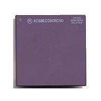
MC68040FE33A Freescale Semiconductor, MC68040FE33A Datasheet - Page 104

MC68040FE33A
Manufacturer Part Number
MC68040FE33A
Description
IC MICROPROCESSOR 32BIT 184-CQFP
Manufacturer
Freescale Semiconductor
Datasheet
1.MC68EC040FE33A.pdf
(442 pages)
Specifications of MC68040FE33A
Processor Type
M680x0 32-Bit
Speed
33MHz
Voltage
5V
Mounting Type
Surface Mount
Package / Case
184-CQFP
Package
184CQFP
Processor Series
M680xx
Core
CPU32
Lead Free Status / RoHS Status
Lead free / RoHS Compliant
Features
-
Lead Free Status / Rohs Status
Details
Available stocks
Company
Part Number
Manufacturer
Quantity
Price
Company:
Part Number:
MC68040FE33A
Manufacturer:
Freescale Semiconductor
Quantity:
10 000
- Current page: 104 of 442
- Download datasheet (4Mb)
5-2
Address Bus
Data Bus
Transfer Type
Transfer Modifier
Transfer Line Number
User-Programmable
Attributes
Read/Write
Transfer Size
Bus Lock
Bus Lock End
Cache Inhibit Out
Transfer Start
Transfer in Progress
Transfer Acknowledge
Transfer Error
Acknowledge
Transfer Cache Inhibit
Transfer Burst Inhibit
Data Latch Enable 1
Snoop Control
Memory Inhibit
Bus Request
Bus Grant
Bus Busy
Cache Disable
MMU Disable 2
Reset In
Reset Out
Interrupt Priority Level 3
Interrupt Pending
Autovector
Processor Status
Bus Clock
Signal Name
UPA1,UPA0 User-defined signals, controlled by the corresponding user attribute bits from
PST3–PST0 Indicates internal processor status.
TLN1,TLN0
Mnemonic
TM2–TM0
IPL2—IPL0 Provides an encoded interrupt level to the processor.
SIZ1,SIZ0
SC1,SC0
TT1,TT0
A31–A0
D31–D0
LOCKE
CIOUT
IPEND
LOCK
RSTO
AVEC
BCLK
MDIS
CDIS
RSTI
DLE
R/W
TEA
TCI
TIP
TBI
BR
BG
TS
TA
MI
BB
Freescale Semiconductor, Inc.
For More Information On This Product,
32-bit address bus used to address any of 4-Gbytes.
32-bit data bus used to transfer up to 32 bits of data per bus transfer.
function code, and acknowledge.
Indicates supplemental information about the access.
line transfer.
the address translation entry.
Identifies the transfer as a read or write.
define the active sections of the data bus.
Indicates a bus transfer is part of a read-modify-write operation, and the
sequence of transfers should not be interrupted.
Indicates the current transfer is the last in a locked sequence of transfers.
Indicates the processor will not cache the current bus transfer.
Indicates the beginning of a bus transfer.
Asserted for the duration of a bus transfer.
Asserted to acknowledge a bus transfer.
Indicates an error condition exists for a bus transfer.
Indicates the current bus transfer should not be cached.
Indicates the slave cannot handle a line burst access.
Alternate clock input used to latch input data when the processor is operating
in DLE mode.
Inhibits memory devices from responding to an alternate master access
during snooping operations.
Asserted by the processor to request bus mastership.
Asserted by an arbiter to grant bus mastership to the processor.
Asserted by the current bus master to indicate it has assumed ownership of
the bus.
Dynamically disables the internal caches to assist emulator support.
Disables the translation mechanism of the MMUs.
Processor reset.
Asserted during execution of a RESET instruction to reset external devices.
Indicates an interrupt is pending.
Used during an interrupt acknowledge transfer to request internal generation
of the vector number.
Clock input used to derive all bus signal timing.
Indicates the general transfer type: normal, MOVE16, alternate logical
Indicates which cache line in a set is being pushed or loaded by the current
Indicates the data transfer size. These signals, together with A0 and A1,
Indicates the snooping operation required during an alternate master access.
Table 5-1. Signal Index
M68040 USER’S MANUAL
Go to: www.freescale.com
Function
MOTOROLA
Related parts for MC68040FE33A
Image
Part Number
Description
Manufacturer
Datasheet
Request
R

Part Number:
Description:
(MC600 Series) INTEGRATED CIRCUITS
Manufacturer:
ETC
Datasheet:
Part Number:
Description:
Manufacturer:
Freescale Semiconductor, Inc
Datasheet:
Part Number:
Description:
Manufacturer:
Freescale Semiconductor, Inc
Datasheet:
Part Number:
Description:
Manufacturer:
Freescale Semiconductor, Inc
Datasheet:
Part Number:
Description:
Manufacturer:
Freescale Semiconductor, Inc
Datasheet:
Part Number:
Description:
Manufacturer:
Freescale Semiconductor, Inc
Datasheet:
Part Number:
Description:
Manufacturer:
Freescale Semiconductor, Inc
Datasheet:
Part Number:
Description:
Manufacturer:
Freescale Semiconductor, Inc
Datasheet:
Part Number:
Description:
Manufacturer:
Freescale Semiconductor, Inc
Datasheet:
Part Number:
Description:
Manufacturer:
Freescale Semiconductor, Inc
Datasheet:
Part Number:
Description:
Manufacturer:
Freescale Semiconductor, Inc
Datasheet:
Part Number:
Description:
Manufacturer:
Freescale Semiconductor, Inc
Datasheet:
Part Number:
Description:
Manufacturer:
Freescale Semiconductor, Inc
Datasheet:
Part Number:
Description:
Manufacturer:
Freescale Semiconductor, Inc
Datasheet:
Part Number:
Description:
Manufacturer:
Freescale Semiconductor, Inc
Datasheet:


