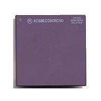
MC68040FE33A Freescale Semiconductor, MC68040FE33A Datasheet - Page 107

MC68040FE33A
Manufacturer Part Number
MC68040FE33A
Description
IC MICROPROCESSOR 32BIT 184-CQFP
Manufacturer
Freescale Semiconductor
Datasheet
1.MC68EC040FE33A.pdf
(442 pages)
Specifications of MC68040FE33A
Processor Type
M680x0 32-Bit
Speed
33MHz
Voltage
5V
Mounting Type
Surface Mount
Package / Case
184-CQFP
Package
184CQFP
Processor Series
M680xx
Core
CPU32
Lead Free Status / RoHS Status
Lead free / RoHS Compliant
Features
-
Lead Free Status / Rohs Status
Details
Available stocks
Company
Part Number
Manufacturer
Quantity
Price
Company:
Part Number:
MC68040FE33A
Manufacturer:
Freescale Semiconductor
Quantity:
10 000
- Current page: 107 of 442
- Download datasheet (4Mb)
applications. Refer to Section 7 Bus Operation for detailed information about the
relationship of the address bus to bus operation and the multiplexed bus mode. Refer to
Appendix A MC68LC040 and Appendix B MC68EC040 for details concerning the CDIS
level and multiplexed bus mode.
5.2 DATA BUS (D31–D0)
These three-state bidirectional signals provide the general-purpose data path between the
M68040 and all other devices. The data bus can transfer 8, 16, or 32 bits of data per bus
transfer. During a burst transfer, the data lines are time-multiplexed to carry all 128 bits of
the burst request using four 32-bit transfers.
The level on CDIS can select a multiplexed bus mode during processor reset, which
allows the data bus and address bus to be physically tied together for multiplexed bus
applications. The level on MDIS can select a data latch mode during processor reset,
which allows the memory interface to specify when the processor should latch input data
through the DLE signal. Section 7 Bus Operation provides detailed information about the
relationship of the data bus to bus operation, the multiplexed bus mode, and the data latch
mode. Refer to Appendix A MC68LC040 and Appendix B MC68EC040 for details
concerning the CDIS level and multiplexed bus mode.
5.3 TRANSFER ATTRIBUTE SIGNALS
The following paragraphs describe the transfer attribute signals, which provide additional
information about the bus transfer. Refer to Section 7 Bus Operation for detailed
information about the relationship of the transfer attribute signals to bus operation.
5.3.1 Transfer Type (TT1, TT0)
The processor drives these three-state bidirectional signals to indicate the type of access
for the current bus transfer. During bus transfers by an alternate bus master, the
processor samples these signals to determine if it should snoop the transfer; only normal
and MOVE16 accesses can be snooped. Table 5-2 lists the definition of the transfer-type
encoding. The acknowledge access (TT1 = 1 and TT0 = 1) is used for both interrupt and
breakpoint acknowledge transfers, and for LPSTOP broadcast cycles on the MC68040V
and MC68EC040V.
MOTOROLA
TT1
0
0
1
1
Freescale Semiconductor, Inc.
For More Information On This Product,
Table 5-2. Transfer-Type Encoding
TT0
0
1
0
1
Go to: www.freescale.com
M68040 USER’S MANUAL
Normal Access
MOVE16 Access
Alternate Logical Function Code Access
Acknowledge Access
Transfer Type
5- 5
Related parts for MC68040FE33A
Image
Part Number
Description
Manufacturer
Datasheet
Request
R

Part Number:
Description:
(MC600 Series) INTEGRATED CIRCUITS
Manufacturer:
ETC
Datasheet:
Part Number:
Description:
Manufacturer:
Freescale Semiconductor, Inc
Datasheet:
Part Number:
Description:
Manufacturer:
Freescale Semiconductor, Inc
Datasheet:
Part Number:
Description:
Manufacturer:
Freescale Semiconductor, Inc
Datasheet:
Part Number:
Description:
Manufacturer:
Freescale Semiconductor, Inc
Datasheet:
Part Number:
Description:
Manufacturer:
Freescale Semiconductor, Inc
Datasheet:
Part Number:
Description:
Manufacturer:
Freescale Semiconductor, Inc
Datasheet:
Part Number:
Description:
Manufacturer:
Freescale Semiconductor, Inc
Datasheet:
Part Number:
Description:
Manufacturer:
Freescale Semiconductor, Inc
Datasheet:
Part Number:
Description:
Manufacturer:
Freescale Semiconductor, Inc
Datasheet:
Part Number:
Description:
Manufacturer:
Freescale Semiconductor, Inc
Datasheet:
Part Number:
Description:
Manufacturer:
Freescale Semiconductor, Inc
Datasheet:
Part Number:
Description:
Manufacturer:
Freescale Semiconductor, Inc
Datasheet:
Part Number:
Description:
Manufacturer:
Freescale Semiconductor, Inc
Datasheet:
Part Number:
Description:
Manufacturer:
Freescale Semiconductor, Inc
Datasheet:


