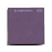
MC68040FE33A Freescale Semiconductor, MC68040FE33A Datasheet - Page 122

MC68040FE33A
Manufacturer Part Number
MC68040FE33A
Description
IC MICROPROCESSOR 32BIT 184-CQFP
Manufacturer
Freescale Semiconductor
Datasheet
1.MC68EC040FE33A.pdf
(442 pages)
Specifications of MC68040FE33A
Processor Type
M680x0 32-Bit
Speed
33MHz
Voltage
5V
Mounting Type
Surface Mount
Package / Case
184-CQFP
Package
184CQFP
Processor Series
M680xx
Core
CPU32
Lead Free Status / RoHS Status
Lead free / RoHS Compliant
Features
-
Lead Free Status / Rohs Status
Details
Available stocks
Company
Part Number
Manufacturer
Quantity
Price
Company:
Part Number:
MC68040FE33A
Manufacturer:
Freescale Semiconductor
Quantity:
10 000
- Current page: 122 of 442
- Download datasheet (4Mb)
6.2 INSTRUCTION SHIFT REGISTER
The M68040 IEEE standard 1149.1A implementation includes a 3-bit instruction shift
register without parity. The register shifts one of eight instructions, which can either select
the test to be performed or access a test data register, or both. Data is transferred from
the instruction shift register to latched decoded outputs during the update-IR state. The
instruction shift register is reset to all ones in the TAP controller test-logic-reset state,
which is equivalent to selecting the BYPASS instruction. During the capture-IR state, the
binary value 001 is loaded into the parallel inputs of the instruction shift register.
The M68040 IEEE standard 1149.1A implementation includes three mandatory public
instructions (BYPASS, SAMPLE/PRELOAD, and EXTEST) and four manufacturer's public
instructions. The four manufacturer’s public instructions provide the capability to disable all
device output drivers, operate the device in a BYPASS configuration without a system
clocking requirement, and select one of two output drive capabilities on a pin-by-pin basis.
The M68040 implementation does not support the optional standard public instructions.
Table 6-1 lists the three bits used in the instruction shift register to decode the instructions
and their related encodings. Note that the least significant bit of the instruction (bit 0) is the
first bit to be shifted into the instruction shift register.
EXTEST, HIGHZ, DRVCTL.T, SHUTDOWN, and PRIVATE have a PCLK and BCLK
restriction. Failure to comply with this restriction results in potential internal damage to the
device (see 6.4 Restrictions). Once the restriction is complied with, SHUTDOWN,
EXTEST, HIGHZ, and DRVCTL.T can be entered regardless of order. The system clocks
(PCLK and BCLK) must be kept running while in the SAMPLE/PRELOAD, DRVCLT.S,
and BYPASS instructions. Failure to do so could result in potential internal damage to the
device.
6.2.1 EXTEST
The external test instruction (EXTEST) selects the 184-bit boundary scan register. This
instruction also activates two internal functions that are intended to protect the device from
potential damage while performing boundary scan operations.
MOTOROLA
Bit 2
0
0
0
0
1
1
1
1
Bit 1
0
0
1
1
0
0
1
1
Table 6-1. IEEE Standard 1149.1A Instructions
Bit 0
0
1
0
1
0
1
0
1
Freescale Semiconductor, Inc.
For More Information On This Product,
Instruction Selected
SAMPLE/PRELOAD
Go to: www.freescale.com
M68040 USER’S MANUAL
SHUTDOWN
DRVCTL.T
DRVCTL.S
PRIVATE
EXTEST
BYPASS
HIGHZ
Test Data Register Accessed
Boundary Scan
Boundary Scan
Boundary Scan
Boundary Scan
Bypass
Bypass
Bypass
Bypass
6- 3
Related parts for MC68040FE33A
Image
Part Number
Description
Manufacturer
Datasheet
Request
R

Part Number:
Description:
(MC600 Series) INTEGRATED CIRCUITS
Manufacturer:
ETC
Datasheet:
Part Number:
Description:
Manufacturer:
Freescale Semiconductor, Inc
Datasheet:
Part Number:
Description:
Manufacturer:
Freescale Semiconductor, Inc
Datasheet:
Part Number:
Description:
Manufacturer:
Freescale Semiconductor, Inc
Datasheet:
Part Number:
Description:
Manufacturer:
Freescale Semiconductor, Inc
Datasheet:
Part Number:
Description:
Manufacturer:
Freescale Semiconductor, Inc
Datasheet:
Part Number:
Description:
Manufacturer:
Freescale Semiconductor, Inc
Datasheet:
Part Number:
Description:
Manufacturer:
Freescale Semiconductor, Inc
Datasheet:
Part Number:
Description:
Manufacturer:
Freescale Semiconductor, Inc
Datasheet:
Part Number:
Description:
Manufacturer:
Freescale Semiconductor, Inc
Datasheet:
Part Number:
Description:
Manufacturer:
Freescale Semiconductor, Inc
Datasheet:
Part Number:
Description:
Manufacturer:
Freescale Semiconductor, Inc
Datasheet:
Part Number:
Description:
Manufacturer:
Freescale Semiconductor, Inc
Datasheet:
Part Number:
Description:
Manufacturer:
Freescale Semiconductor, Inc
Datasheet:
Part Number:
Description:
Manufacturer:
Freescale Semiconductor, Inc
Datasheet:


