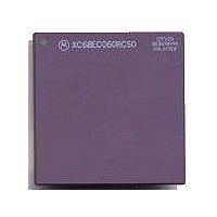
MC68040FE33A Freescale Semiconductor, MC68040FE33A Datasheet - Page 143

MC68040FE33A
Manufacturer Part Number
MC68040FE33A
Description
IC MICROPROCESSOR 32BIT 184-CQFP
Manufacturer
Freescale Semiconductor
Datasheet
1.MC68EC040FE33A.pdf
(442 pages)
Specifications of MC68040FE33A
Processor Type
M680x0 32-Bit
Speed
33MHz
Voltage
5V
Mounting Type
Surface Mount
Package / Case
184-CQFP
Package
184CQFP
Processor Series
M680xx
Core
CPU32
Lead Free Status / RoHS Status
Lead free / RoHS Compliant
Features
-
Lead Free Status / Rohs Status
Details
Available stocks
Company
Part Number
Manufacturer
Quantity
Price
Company:
Part Number:
MC68040FE33A
Manufacturer:
Freescale Semiconductor
Quantity:
10 000
- Current page: 143 of 442
- Download datasheet (4Mb)
SECTION 7
BUS OPERATION
The M68040 bus interface supports synchronous data transfers between the processor
and other devices in the system. This section provides a functional description of the bus,
the signals that control the bus, and the bus cycles provided for data transfer operations.
Operation of the bus is defined for transfers initiated by the processor as a bus master and
for transfers initiated by an alternate bus master, which the processor snoops as a slave
device. Descriptions of the error and halt conditions, bus arbitration, and the reset
operation are also included. For timing specifications, refer to Section 11 MC68040
Electrical and Thermal Characteristics.
7.1 BUS CHARACTERISTICS
The M68040 uses the address bus (A31–A0) to specify the address for a data transfer
and the data bus (D31–D0) to transfer the data. Control signals indicate the beginning and
type of a bus cycle as well as the address space and size of the transfer. The selected
device then controls the length of the cycle by terminating it using the control signals.
The M68040 uses two clocks to generate timing: a processor clock (PCLK) and a bus
clock (BCLK). The PCLK signal is twice the frequency of the BCLK signal and is internally
phase-locked to BCLK. PCLK is also distributed throughout the device to generate
additional timing for additional edges for internal logic blocks and has no bearing on bus
timing. The use of dual clock inputs allows the bus interface to operate at half the speed of
the internal logic of the processor, requiring less stringent memory interface requirements.
Since the rising edge of BCLK is used as the reference point for the phase-locked loop
(PLL), all timing specifications are referenced to this edge.
Figure 7-1 illustrates the general relationship between the two clock signals and most
input and output signals. The rising edge of the internally phase-locked PCLK is aligned
with the rising edge of BCLK, and the two PCLK cycles corresponding to each BCLK cycle
are divided into four states, T1–T4. Most outputs change during state T4, whether
transitioning between a driven and high-impedance state or switching between assert and
MOTOROLA
For the MC68040V, MC68LC040, and MC68EC040 ignore all
references to floating-point. For the MC68EC040 and
MC68EC040V ignore all references to the memory
management unit (MMU). Special modes of operation do not
apply to these devices. Refer to Appendix A MC68LC040 and
Appendix B MC68EC040 for details.
Freescale Semiconductor, Inc.
For More Information On This Product,
Go to: www.freescale.com
M68040 USER’S MANUAL
NOTE
7- 1
Related parts for MC68040FE33A
Image
Part Number
Description
Manufacturer
Datasheet
Request
R

Part Number:
Description:
(MC600 Series) INTEGRATED CIRCUITS
Manufacturer:
ETC
Datasheet:
Part Number:
Description:
Manufacturer:
Freescale Semiconductor, Inc
Datasheet:
Part Number:
Description:
Manufacturer:
Freescale Semiconductor, Inc
Datasheet:
Part Number:
Description:
Manufacturer:
Freescale Semiconductor, Inc
Datasheet:
Part Number:
Description:
Manufacturer:
Freescale Semiconductor, Inc
Datasheet:
Part Number:
Description:
Manufacturer:
Freescale Semiconductor, Inc
Datasheet:
Part Number:
Description:
Manufacturer:
Freescale Semiconductor, Inc
Datasheet:
Part Number:
Description:
Manufacturer:
Freescale Semiconductor, Inc
Datasheet:
Part Number:
Description:
Manufacturer:
Freescale Semiconductor, Inc
Datasheet:
Part Number:
Description:
Manufacturer:
Freescale Semiconductor, Inc
Datasheet:
Part Number:
Description:
Manufacturer:
Freescale Semiconductor, Inc
Datasheet:
Part Number:
Description:
Manufacturer:
Freescale Semiconductor, Inc
Datasheet:
Part Number:
Description:
Manufacturer:
Freescale Semiconductor, Inc
Datasheet:
Part Number:
Description:
Manufacturer:
Freescale Semiconductor, Inc
Datasheet:
Part Number:
Description:
Manufacturer:
Freescale Semiconductor, Inc
Datasheet:


