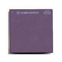
MC68040FE33A Freescale Semiconductor, MC68040FE33A Datasheet - Page 151

MC68040FE33A
Manufacturer Part Number
MC68040FE33A
Description
IC MICROPROCESSOR 32BIT 184-CQFP
Manufacturer
Freescale Semiconductor
Datasheet
1.MC68EC040FE33A.pdf
(442 pages)
Specifications of MC68040FE33A
Processor Type
M680x0 32-Bit
Speed
33MHz
Voltage
5V
Mounting Type
Surface Mount
Package / Case
184-CQFP
Package
184CQFP
Processor Series
M680xx
Core
CPU32
Lead Free Status / RoHS Status
Lead free / RoHS Compliant
Features
-
Lead Free Status / Rohs Status
Details
Available stocks
Company
Part Number
Manufacturer
Quantity
Price
Company:
Part Number:
MC68040FE33A
Manufacturer:
Freescale Semiconductor
Quantity:
10 000
- Current page: 151 of 442
- Download datasheet (4Mb)
The combination of operand size and alignment determines the number of bus cycles
required to perform a particular memory access. Table 7-3 lists the number of bus cycles
required for different operand sizes with all possible alignment conditions for read and
write cycles. The table confirms that alignment significantly affects bus cycle throughput
for noncachable accesses. For example, in Figure 7-5 the misaligned long-word operand
took three bus cycles because the byte offset = $1. If the byte offset = $0, then it would
have taken one bus cycle. The M68040 system designer and programmer should account
for these effects, particularly in time-critical applications.
The processor always prefetches instructions by reading a long word from a half-line
address (A2–A0 = $0), regardless of alignment. When the required instruction begins at
the second long word, the processor attempts to fetch the entire half-line (two long words)
although the second long word contains the required instruction.
7.4 PROCESSOR DATA TRANSFERS
The transfer of data between the processor and other devices involves the address bus,
data bus, and control signals. The address and data buses are normally parallel,
nonmultiplexed buses, supporting byte, word, long-word, and line (16-byte) bus cycles.
Line transfers are normally performed using an efficient burst transfer, which provides an
initial address and time-multiplexes the data bus to transfer four long words of information
to or from the slave device. Slave devices that do not support bursting can burst-inhibit the
first long word of a line transfer, forcing the bus master to complete the access using three
additional long-word bus cycles. All bus input and output signals are synchronous to the
rising edge of the BCLK signal. The M68040 moves data on the bus by issuing control
signals and using a handshake protocol to ensure correct data movement. The following
paragraphs describe the bus cycles for byte, word, long-word, and line read, write, and
read-modify-write transfers.
MOTOROLA
*Where the byte offset (A1 and A0) equals this encoding.
Instruction
Byte Operand
Word Operand
Long-Word Operand
Noncachable and Write-Through Bus Cycles
Table 7-3. Memory Alignment Influence on
Freescale Semiconductor, Inc.
Transfer Size
For More Information On This Product,
Go to: www.freescale.com
M68040 USER’S MANUAL
$0 *
1
1
1
1
Number of Bus Cycles
N/A
$1 *
2
3
1
$2 *
N/A
1
1
2
$3 *
N/A
2
3
1
7- 9
Related parts for MC68040FE33A
Image
Part Number
Description
Manufacturer
Datasheet
Request
R

Part Number:
Description:
(MC600 Series) INTEGRATED CIRCUITS
Manufacturer:
ETC
Datasheet:
Part Number:
Description:
Manufacturer:
Freescale Semiconductor, Inc
Datasheet:
Part Number:
Description:
Manufacturer:
Freescale Semiconductor, Inc
Datasheet:
Part Number:
Description:
Manufacturer:
Freescale Semiconductor, Inc
Datasheet:
Part Number:
Description:
Manufacturer:
Freescale Semiconductor, Inc
Datasheet:
Part Number:
Description:
Manufacturer:
Freescale Semiconductor, Inc
Datasheet:
Part Number:
Description:
Manufacturer:
Freescale Semiconductor, Inc
Datasheet:
Part Number:
Description:
Manufacturer:
Freescale Semiconductor, Inc
Datasheet:
Part Number:
Description:
Manufacturer:
Freescale Semiconductor, Inc
Datasheet:
Part Number:
Description:
Manufacturer:
Freescale Semiconductor, Inc
Datasheet:
Part Number:
Description:
Manufacturer:
Freescale Semiconductor, Inc
Datasheet:
Part Number:
Description:
Manufacturer:
Freescale Semiconductor, Inc
Datasheet:
Part Number:
Description:
Manufacturer:
Freescale Semiconductor, Inc
Datasheet:
Part Number:
Description:
Manufacturer:
Freescale Semiconductor, Inc
Datasheet:
Part Number:
Description:
Manufacturer:
Freescale Semiconductor, Inc
Datasheet:


