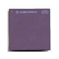
MC68040FE33A Freescale Semiconductor, MC68040FE33A Datasheet - Page 168

MC68040FE33A
Manufacturer Part Number
MC68040FE33A
Description
IC MICROPROCESSOR 32BIT 184-CQFP
Manufacturer
Freescale Semiconductor
Datasheet
1.MC68EC040FE33A.pdf
(442 pages)
Specifications of MC68040FE33A
Processor Type
M680x0 32-Bit
Speed
33MHz
Voltage
5V
Mounting Type
Surface Mount
Package / Case
184-CQFP
Package
184CQFP
Processor Series
M680xx
Core
CPU32
Lead Free Status / RoHS Status
Lead free / RoHS Compliant
Features
-
Lead Free Status / Rohs Status
Details
Available stocks
Company
Part Number
Manufacturer
Quantity
Price
Company:
Part Number:
MC68040FE33A
Manufacturer:
Freescale Semiconductor
Quantity:
10 000
- Current page: 168 of 442
- Download datasheet (4Mb)
7.4.5 Read-Modify-Write Transfers (Locked Transfers)
The read-modify-write transfer performs a read, conditionally modifies the data in the
processor, and writes the data out to memory. In the M68040, this operation can be
indivisible, providing semaphore capabilities for multiprocessor systems. During the entire
read-modify-write sequence, the M68040 asserts the LOCK signal to indicate that an
indivisible operation is occurring and asserts the LOCKE signal for the last transfer to
indicate completion of the locked sequence. The external arbiter can use the LOCK and
LOCKE signals to prevent arbitration of the bus during locked processor sequences.
External bus arbitrations can use LOCKE to support bus arbitration between consecutive
read-modify-write cycles. A read-modify-write operation is treated as noncachable. If the
access hits in the data cache, it invalidates a matching valid entry and pushes a matching
dirty entry. The read-modify-write transfer begins after the line push (if required) is
complete; however, LOCK may assert during the line push bus cycle.
The TAS, CAS, and CAS2 instructions are the only M68040 instructions that utilize read-
modify-write transfers. Some page descriptor updates during translation table searches
also use read-modify-write transfers. Refer to Section 3 Memory Management Unit
(Except MC68EC040 and MC68EC040V) for information about table searches.
The read-modify-write transfer for the CAS and CAS2 instructions in the M68040 differs
from those used by previous members of the M68000 family. If an operand does not
match one of these instructions, the M68040 still executes a single write transfer to
terminate the locked sequence with LOCKE asserted. For the CAS instruction, the value
read from memory is written back; for the CAS2 instruction, the second operand read is
written back. Figure 7-18 illustrates a functional timing diagram for a TAS instruction read-
modify-write bus transfer.
Clock 1 (C1)
7-26
The read cycle starts in C1. During the first half of C1, the processor places valid values
on the address bus and transfer attributes. LOCK is asserted to identify a locked read-
modify-write bus cycle. For user and supervisor mode accesses, which the
corresponding memory unit translates, the UPAx signals are driven with the values from
the matching U1 and U0 bits. The TTx and TMx signals identify the specific access
type. R/W is driven high for a read cycle. CIOUT is asserted if the access is identified as
noncachable. The processor asserts TS during C1 to indicate the beginning of a bus
cycle. If not already asserted from a previous bus cycle, the TIP signal is also asserted
at this time to indicate that a bus cycle is active. Refer to Section 3 Memory
Management Unit (Except MC68EC040 and MC68EC040V) for information on the
M68040 and MC68LC040 memory units and Appendix B MC68EC040 for information
on the MC68EC040 memory unit.
Freescale Semiconductor, Inc.
For More Information On This Product,
M68040 USER’S MANUAL
Go to: www.freescale.com
MOTOROLA
Related parts for MC68040FE33A
Image
Part Number
Description
Manufacturer
Datasheet
Request
R

Part Number:
Description:
(MC600 Series) INTEGRATED CIRCUITS
Manufacturer:
ETC
Datasheet:
Part Number:
Description:
Manufacturer:
Freescale Semiconductor, Inc
Datasheet:
Part Number:
Description:
Manufacturer:
Freescale Semiconductor, Inc
Datasheet:
Part Number:
Description:
Manufacturer:
Freescale Semiconductor, Inc
Datasheet:
Part Number:
Description:
Manufacturer:
Freescale Semiconductor, Inc
Datasheet:
Part Number:
Description:
Manufacturer:
Freescale Semiconductor, Inc
Datasheet:
Part Number:
Description:
Manufacturer:
Freescale Semiconductor, Inc
Datasheet:
Part Number:
Description:
Manufacturer:
Freescale Semiconductor, Inc
Datasheet:
Part Number:
Description:
Manufacturer:
Freescale Semiconductor, Inc
Datasheet:
Part Number:
Description:
Manufacturer:
Freescale Semiconductor, Inc
Datasheet:
Part Number:
Description:
Manufacturer:
Freescale Semiconductor, Inc
Datasheet:
Part Number:
Description:
Manufacturer:
Freescale Semiconductor, Inc
Datasheet:
Part Number:
Description:
Manufacturer:
Freescale Semiconductor, Inc
Datasheet:
Part Number:
Description:
Manufacturer:
Freescale Semiconductor, Inc
Datasheet:
Part Number:
Description:
Manufacturer:
Freescale Semiconductor, Inc
Datasheet:


