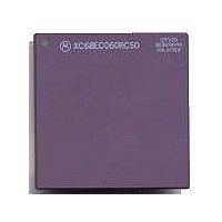
MC68040FE33A Freescale Semiconductor, MC68040FE33A Datasheet - Page 295

MC68040FE33A
Manufacturer Part Number
MC68040FE33A
Description
IC MICROPROCESSOR 32BIT 184-CQFP
Manufacturer
Freescale Semiconductor
Datasheet
1.MC68EC040FE33A.pdf
(442 pages)
Specifications of MC68040FE33A
Processor Type
M680x0 32-Bit
Speed
33MHz
Voltage
5V
Mounting Type
Surface Mount
Package / Case
184-CQFP
Package
184CQFP
Processor Series
M680xx
Core
CPU32
Lead Free Status / RoHS Status
Lead free / RoHS Compliant
Features
-
Lead Free Status / Rohs Status
Details
Available stocks
Company
Part Number
Manufacturer
Quantity
Price
Company:
Part Number:
MC68040FE33A
Manufacturer:
Freescale Semiconductor
Quantity:
10 000
- Current page: 295 of 442
- Download datasheet (4Mb)
example, if an execution time is listed as 2
time is one for a total execution time of three. The instruction can stall for two clocks
without delaying the instruction execution time.
The <ea> calculate and execute stages operate in an interlocked manner for all
instructions using the brief and full extension word formats. If an instruction using one of
these formats is stalled for more than N
stage, a similar increase in the <ea> calculate time will result. For example, if the
execution time listed is 2
calculate time increases by one clock (3 – 1 = 2
they are system dependent and do not affect either <ea> calculate or execute stages of
the pipeline.
Not all addressing modes listed in the following tables for an instruction are valid for all
variations of the instruction. For example, the table for the integer ADD instruction lists
times for both ADD <ea>,Dn and ADD Dn,<ea>. All addressing modes listed are valid for
ADD <ea>,Dn. For ADD Dn,<ea> the following invalid modes should be ignored: An,
(d
M68000 Family Programmer's Reference Manual for a complete summary of valid
instruction and addressing mode combinations. The instruction timings are based on the
following suppositions unless otherwise noted:
10-4
16
1. All timings are related to BCLK cycles and are for BR = An or suppressed. For BR =
2. All memory accesses hit in the caches; no table searches occur as a result of ATC
3. All accesses are aligned to a byte boundary that is a multiple of the operand size.
4. The integer execution times for floating-point instructions assume that the floating-
,PC), #<xxx>, (d
PC, 1 and 1
noted. For memory indirect postindexed with suppressed index — ([bd,BR],Xn) or
([bd,BR],Xn,od) with Xn suppressed — times are the same as for memory indirect
preindexed with suppressed index — ([bd,BR,Xn]) or ([bd,BR,Xn],od) with Xn
suppressed.
misses except for the operand accesses for the CAS, CAS2, and TAS instructions.
These accesses are implicitly noncachable and force external bus accesses. It is
assumed that external memory has a zero-wait state in this case and that the bus is
granted to the M68040.
The result increases access time equal to the number of clocks for the memory
access (first bus cycle if the operand access results in a line memory access) if
aligned accesses miss in the data cache. As an approximation, this time should be
added to the execution time for each operand fetch generated by the instruction.
For instance, the timing for all long-word accesses assumes that the operands are
on long-word boundaries.
point unit (FPU) is idle.
L
clocks to the <ea> calculate and execution times unless otherwise
8
,PC,Xn), and modes with BR = PC. Refer to the M68000PM/AD,
Freescale Semiconductor, Inc.
L
For More Information On This Product,
+ 1 and the instruction stalls for three clocks, then the <ea>
M68040 USER’S MANUAL
Go to: www.freescale.com
L
clocks waiting to begin execution in the execute
L
+ 1, the lead time is two clocks and the base
L
). Write-back times are not listed because
MOTOROLA
Related parts for MC68040FE33A
Image
Part Number
Description
Manufacturer
Datasheet
Request
R

Part Number:
Description:
(MC600 Series) INTEGRATED CIRCUITS
Manufacturer:
ETC
Datasheet:
Part Number:
Description:
Manufacturer:
Freescale Semiconductor, Inc
Datasheet:
Part Number:
Description:
Manufacturer:
Freescale Semiconductor, Inc
Datasheet:
Part Number:
Description:
Manufacturer:
Freescale Semiconductor, Inc
Datasheet:
Part Number:
Description:
Manufacturer:
Freescale Semiconductor, Inc
Datasheet:
Part Number:
Description:
Manufacturer:
Freescale Semiconductor, Inc
Datasheet:
Part Number:
Description:
Manufacturer:
Freescale Semiconductor, Inc
Datasheet:
Part Number:
Description:
Manufacturer:
Freescale Semiconductor, Inc
Datasheet:
Part Number:
Description:
Manufacturer:
Freescale Semiconductor, Inc
Datasheet:
Part Number:
Description:
Manufacturer:
Freescale Semiconductor, Inc
Datasheet:
Part Number:
Description:
Manufacturer:
Freescale Semiconductor, Inc
Datasheet:
Part Number:
Description:
Manufacturer:
Freescale Semiconductor, Inc
Datasheet:
Part Number:
Description:
Manufacturer:
Freescale Semiconductor, Inc
Datasheet:
Part Number:
Description:
Manufacturer:
Freescale Semiconductor, Inc
Datasheet:
Part Number:
Description:
Manufacturer:
Freescale Semiconductor, Inc
Datasheet:


