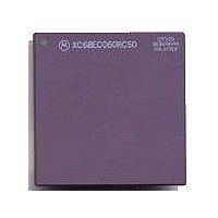
MC68040FE33A Freescale Semiconductor, MC68040FE33A Datasheet - Page 42

MC68040FE33A
Manufacturer Part Number
MC68040FE33A
Description
IC MICROPROCESSOR 32BIT 184-CQFP
Manufacturer
Freescale Semiconductor
Datasheet
1.MC68EC040FE33A.pdf
(442 pages)
Specifications of MC68040FE33A
Processor Type
M680x0 32-Bit
Speed
33MHz
Voltage
5V
Mounting Type
Surface Mount
Package / Case
184-CQFP
Package
184CQFP
Processor Series
M680xx
Core
CPU32
Lead Free Status / RoHS Status
Lead free / RoHS Compliant
Features
-
Lead Free Status / Rohs Status
Details
Available stocks
Company
Part Number
Manufacturer
Quantity
Price
Company:
Part Number:
MC68040FE33A
Manufacturer:
Freescale Semiconductor
Quantity:
10 000
- Current page: 42 of 442
- Download datasheet (4Mb)
SECTION 2
INTEGER UNIT
This section describes the organization of the M68040 integer unit (IU) and presents a
brief description of the associated registers. Refer to Section 3 Memory Management
Unit (Except MC68EC040 and MC68EC040V) for details concerning the memory
management unit (MMU) programming model, and to Section 9 Floating-Point Unit
(MC68040 Only) for details concerning the floating-point unit (FPU) programming model.
2.1 INTEGER UNIT PIPELINE
The IU carries out logical and arithmetic operations using six separate subunits. Each unit
is dedicated to a different stage of the IU pipeline, handling a total of six separate
instructions simultaneously. Pipelining is a technique that overlaps the processing of
different parts of several instructions. Pipelining simulates an assembly line with the IU
containing a number of instructions in different phases of processing. The IU pipeline
consists of six stages:
The pipeline contains special shadow registers that can begin processing future
instructions for conditional branches while the main pipeline is processing current
instructions. The <ea> calculate stage eliminates pipeline blockage for instructions with
postincrement, postdecrement, or immediate add and load to address register for updates
that occur in the <ea> calculate stage. The write-back stage can write data over the
system bus to store a result in external memory or directly to on-chip caches. These write-
backs to memory can be deferred until the most opportune moment because of the
M68040 bus interface. Figure 2-1 illustrates the IU pipeline.
MOTOROLA
1. Instruction Fetch—Fetching an instruction from memory.
2. Decode—Converting an instruction into micro-instructions.
3. <ea> Calculate—If the instruction calls for data from memory, the location of the
4. <ea> Fetch—Data is fetched from memory.
5. Execute—The data is manipulated during execution.
6. Write-Back—The result of the computation is written back to on-chip caches or
data, its memory address is calculated.
external memory.
Freescale Semiconductor, Inc.
For More Information On This Product,
Go to: www.freescale.com
M68040 USER’S MANUAL
2- 1
Related parts for MC68040FE33A
Image
Part Number
Description
Manufacturer
Datasheet
Request
R

Part Number:
Description:
(MC600 Series) INTEGRATED CIRCUITS
Manufacturer:
ETC
Datasheet:
Part Number:
Description:
Manufacturer:
Freescale Semiconductor, Inc
Datasheet:
Part Number:
Description:
Manufacturer:
Freescale Semiconductor, Inc
Datasheet:
Part Number:
Description:
Manufacturer:
Freescale Semiconductor, Inc
Datasheet:
Part Number:
Description:
Manufacturer:
Freescale Semiconductor, Inc
Datasheet:
Part Number:
Description:
Manufacturer:
Freescale Semiconductor, Inc
Datasheet:
Part Number:
Description:
Manufacturer:
Freescale Semiconductor, Inc
Datasheet:
Part Number:
Description:
Manufacturer:
Freescale Semiconductor, Inc
Datasheet:
Part Number:
Description:
Manufacturer:
Freescale Semiconductor, Inc
Datasheet:
Part Number:
Description:
Manufacturer:
Freescale Semiconductor, Inc
Datasheet:
Part Number:
Description:
Manufacturer:
Freescale Semiconductor, Inc
Datasheet:
Part Number:
Description:
Manufacturer:
Freescale Semiconductor, Inc
Datasheet:
Part Number:
Description:
Manufacturer:
Freescale Semiconductor, Inc
Datasheet:
Part Number:
Description:
Manufacturer:
Freescale Semiconductor, Inc
Datasheet:
Part Number:
Description:
Manufacturer:
Freescale Semiconductor, Inc
Datasheet:


