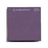
MC68040FE33A Freescale Semiconductor, MC68040FE33A Datasheet - Page 44

MC68040FE33A
Manufacturer Part Number
MC68040FE33A
Description
IC MICROPROCESSOR 32BIT 184-CQFP
Manufacturer
Freescale Semiconductor
Datasheet
1.MC68EC040FE33A.pdf
(442 pages)
Specifications of MC68040FE33A
Processor Type
M680x0 32-Bit
Speed
33MHz
Voltage
5V
Mounting Type
Surface Mount
Package / Case
184-CQFP
Package
184CQFP
Processor Series
M680xx
Core
CPU32
Lead Free Status / RoHS Status
Lead free / RoHS Compliant
Features
-
Lead Free Status / Rohs Status
Details
Available stocks
Company
Part Number
Manufacturer
Quantity
Price
Company:
Part Number:
MC68040FE33A
Manufacturer:
Freescale Semiconductor
Quantity:
10 000
- Current page: 44 of 442
- Download datasheet (4Mb)
effective address. Also, some instructions access multiple memory operands and initiate
fetches for each operand.
The instruction finishes execution in the execute stage. Instructions with write-back
operands to memory generate pending write accesses that are passed to the write-back
stage. The write occurs to the data memory unit if it is not busy. If the following instruction,
which is in the <ea> fetch stage, requires an operand fetch, the write-back stalls in the
write-back stage since it is at a lower priority. The write-back can stall indefinitely until
either the data memory unit is free or another write is pending from the execution stage.
Figure 2-2 illustrates a write cycle, which begins in the IU pipeline. The IU stores the
logical address and data for a write operation in a temporary holding register (WB3). Write
operation control passes from the IU to the data memory unit once the data memory unit
is idle. When the data memory unit receives the logical address and data from the IU, it
stores the logical address and data to a second temporary holding register (WB2). The
data memory unit then translates the logical address into a physical address. If the
address translation is successful, the data memory unit either stores an address
translation in the data cache (write hit) or passes it to the bus controller (write-through with
write miss). Once the bus controller is ready to execute the external write operation, it
multiplexes the data to the correct data byte lanes and stores the multiplexed data and
physical address into a third holding register (WB1). WB1 is used in the actual write
operation seen on the address and data buses. Appendix B MC68EC040 contains details
on address translation in the MC68EC040.
MOTOROLA
INSTRUCTION
INTEGER UNIT
CALCULATE
BACK (WB3)
EXECUTE
DECODE
WRITE-
FETCH
FETCH
<ea>
<ea>
Figure 2-2. Write-Back Cycle Block Diagram
Freescale Semiconductor, Inc.
For More Information On This Product,
INSTRUCTION MEMORY UNIT
DATA
WB2
ATC
DATA MEMORY UNIT
Go to: www.freescale.com
M68040 USER’S MANUAL
DATA CACHE
PHYSICAL ADDRESS
CACHE/SNOOP
CONTROLLER
DATA MMU/
DATA MUX
BUFFER
CONTROLLER
PUSH
WB1
BUS
ADDRESS
CONTROL
SIGNALS
DATA
BUS
BUS
BUS
2- 3
Related parts for MC68040FE33A
Image
Part Number
Description
Manufacturer
Datasheet
Request
R

Part Number:
Description:
(MC600 Series) INTEGRATED CIRCUITS
Manufacturer:
ETC
Datasheet:
Part Number:
Description:
Manufacturer:
Freescale Semiconductor, Inc
Datasheet:
Part Number:
Description:
Manufacturer:
Freescale Semiconductor, Inc
Datasheet:
Part Number:
Description:
Manufacturer:
Freescale Semiconductor, Inc
Datasheet:
Part Number:
Description:
Manufacturer:
Freescale Semiconductor, Inc
Datasheet:
Part Number:
Description:
Manufacturer:
Freescale Semiconductor, Inc
Datasheet:
Part Number:
Description:
Manufacturer:
Freescale Semiconductor, Inc
Datasheet:
Part Number:
Description:
Manufacturer:
Freescale Semiconductor, Inc
Datasheet:
Part Number:
Description:
Manufacturer:
Freescale Semiconductor, Inc
Datasheet:
Part Number:
Description:
Manufacturer:
Freescale Semiconductor, Inc
Datasheet:
Part Number:
Description:
Manufacturer:
Freescale Semiconductor, Inc
Datasheet:
Part Number:
Description:
Manufacturer:
Freescale Semiconductor, Inc
Datasheet:
Part Number:
Description:
Manufacturer:
Freescale Semiconductor, Inc
Datasheet:
Part Number:
Description:
Manufacturer:
Freescale Semiconductor, Inc
Datasheet:
Part Number:
Description:
Manufacturer:
Freescale Semiconductor, Inc
Datasheet:


