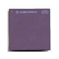
MC68040FE33A Freescale Semiconductor, MC68040FE33A Datasheet - Page 52

MC68040FE33A
Manufacturer Part Number
MC68040FE33A
Description
IC MICROPROCESSOR 32BIT 184-CQFP
Manufacturer
Freescale Semiconductor
Datasheet
1.MC68EC040FE33A.pdf
(442 pages)
Specifications of MC68040FE33A
Processor Type
M680x0 32-Bit
Speed
33MHz
Voltage
5V
Mounting Type
Surface Mount
Package / Case
184-CQFP
Package
184CQFP
Processor Series
M680xx
Core
CPU32
Lead Free Status / RoHS Status
Lead free / RoHS Compliant
Features
-
Lead Free Status / Rohs Status
Details
Available stocks
Company
Part Number
Manufacturer
Quantity
Price
Company:
Part Number:
MC68040FE33A
Manufacturer:
Freescale Semiconductor
Quantity:
10 000
- Current page: 52 of 442
- Download datasheet (4Mb)
logical address bits. If the translation is resident, the MMU provides the physical address
to the cache controller, which determines if the instruction or data being accessed is
cached. The cache controller uses the lower address bits to index into memory. An
external bus cycle is performed only when explicitly requested by the cache controller.
When the translation is not in the ATC, the MMU searches the translation tables in
memory for the translation information. Microcode and dedicated logic perform the
address calculations and bus cycles required for this search.
3.1 MEMORY MANAGEMENT PROGRAMMING MODEL
The memory management programming model is part of the supervisor programming
model for the M68040. The eight registers that control and provide status information for
address translation in the M68040 are: the user root pointer register (URP), the supervisor
root pointer register (SRP), the translation control register (TCR), four independent
transparent translation registers (ITT0, ITT1, DTT0, and DTT1), and the MMU status
register (MMUSR). Only programs that execute in the supervisor mode can directly
access these registers. Figure 3-2 illustrates the memory management programming
model.
3.1.1 User and Supervisor Root Pointer Registers
The SRP and URP registers each contain the physical address of the translation table’s
root, which the MMU uses for supervisor and user accesses, respectively. The URP points
to the translation table for the current user task. When a new task begins execution, the
operating system typically writes a new root pointer to the URP. A new translation table
address implies that the contents of the ATCs may no longer be valid. A PFLUSH
instruction should be executed to flush the ATCs before loading a new root pointer value,
if necessary. Figure 3-3 illustrates the format of the 32-bit URP and SRP registers. Bits 8–
MOTOROLA
31
31
31
31
31
31
31
Figure 3-2. Memory Management Programming Model
Freescale Semiconductor, Inc.
15
For More Information On This Product,
Go to: www.freescale.com
M68040 USER'S MANUAL
0
0
0
0
0
0
0
0
URP
SRP
DTTR0
DTTR1
ITTR0
ITTR1
MMUSR
TCR
USER ROOT POINTER REGISTER
SUPERVISOR ROOT POINTER REGISTER
TRANSLATION CONTROL REGISTER
DATA TRANSPARENT TRANSLATION REGISTER 0
DATA TRANSPARENT TRANSLATION REGISTER 1
INSTRUCTION TRANSPARENT TRANSLATION
REGISTER 0
INSTRUCTION TRANSPARENT TRANSLATION
REGISTER 1
MMU STATUS REGISTER
3- 3
Related parts for MC68040FE33A
Image
Part Number
Description
Manufacturer
Datasheet
Request
R

Part Number:
Description:
(MC600 Series) INTEGRATED CIRCUITS
Manufacturer:
ETC
Datasheet:
Part Number:
Description:
Manufacturer:
Freescale Semiconductor, Inc
Datasheet:
Part Number:
Description:
Manufacturer:
Freescale Semiconductor, Inc
Datasheet:
Part Number:
Description:
Manufacturer:
Freescale Semiconductor, Inc
Datasheet:
Part Number:
Description:
Manufacturer:
Freescale Semiconductor, Inc
Datasheet:
Part Number:
Description:
Manufacturer:
Freescale Semiconductor, Inc
Datasheet:
Part Number:
Description:
Manufacturer:
Freescale Semiconductor, Inc
Datasheet:
Part Number:
Description:
Manufacturer:
Freescale Semiconductor, Inc
Datasheet:
Part Number:
Description:
Manufacturer:
Freescale Semiconductor, Inc
Datasheet:
Part Number:
Description:
Manufacturer:
Freescale Semiconductor, Inc
Datasheet:
Part Number:
Description:
Manufacturer:
Freescale Semiconductor, Inc
Datasheet:
Part Number:
Description:
Manufacturer:
Freescale Semiconductor, Inc
Datasheet:
Part Number:
Description:
Manufacturer:
Freescale Semiconductor, Inc
Datasheet:
Part Number:
Description:
Manufacturer:
Freescale Semiconductor, Inc
Datasheet:
Part Number:
Description:
Manufacturer:
Freescale Semiconductor, Inc
Datasheet:


