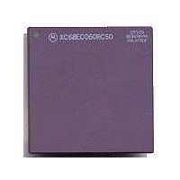
MC68040FE33A Freescale Semiconductor, MC68040FE33A Datasheet - Page 54

MC68040FE33A
Manufacturer Part Number
MC68040FE33A
Description
IC MICROPROCESSOR 32BIT 184-CQFP
Manufacturer
Freescale Semiconductor
Datasheet
1.MC68EC040FE33A.pdf
(442 pages)
Specifications of MC68040FE33A
Processor Type
M680x0 32-Bit
Speed
33MHz
Voltage
5V
Mounting Type
Surface Mount
Package / Case
184-CQFP
Package
184CQFP
Processor Series
M680xx
Core
CPU32
Lead Free Status / RoHS Status
Lead free / RoHS Compliant
Features
-
Lead Free Status / Rohs Status
Details
Available stocks
Company
Part Number
Manufacturer
Quantity
Price
Company:
Part Number:
MC68040FE33A
Manufacturer:
Freescale Semiconductor
Quantity:
10 000
- Current page: 54 of 442
- Download datasheet (4Mb)
3.1.3 Transparent Translation Registers
The data transparent translation registers (DTTR0 and DTTR1) and instruction
transparent translation registers (ITTR0 and ITTR1) are 32-bit registers that define blocks
of logical address space. The TTRs operate independently of the E-bit in the TCR and the
state of the MDIS signal. Data transfers to and from these registers are long-word
transfers. The TTR fields are defined following Figure 3-5, which illustrates TTR format.
Bits 12–10, 7, 4, 3, 1, and 0 always read as zero.
Logical Address Base
Logical Address Mask
E—Enable
S—Supervisor Mode
U0, U1—User Page Attributes
MOTOROLA
31
LOGICAL ADDRESS BASE
This 8-bit field is compared with address bits A31–A24. Addresses that match in this
comparison (and are otherwise eligible) are transparently translated.
Since this 8-bit field contains a mask for the Logical Address Mask field, setting a bit in
this field causes the corresponding bit in the Logical Address Base field to be ignored.
Blocks of memory larger than 16 Mbytes can be transparently translated by setting
some of the logical address mask bits to ones. The low-order bits of this field can be set
to define contiguous blocks larger than 16 Mbytes.
This bit enables or disables transparent translation of the block defined by this register:
This field specifies the way FC2 is used in matching an address:
The user defines these bits, and the M68040 does not interpret them. U0 and U1 are
echoed to the UPA0 and UPA1 signals, respectively, if an external bus transfer results
from an access. These bits can be programmed by the user to support external
addressing, bus snooping, or other applications.
0 = Transparent translation disabled
1 = Transparent translation enabled
00 = Match only if FC2 = 0 (user mode access)
01 = Match only if FC2 = 1 (supervisor mode access)
1X = Ignore FC2 when matching
24
Figure 3-5. Transparent Translation Register Format
23
LOGICAL ADDRESS MASK
Freescale Semiconductor, Inc.
For More Information On This Product,
16
Go to: www.freescale.com
M68040 USER'S MANUAL
15
E
S-FIELD
14
13
12
0
11
0
10
0
U1 U 0
9
8
7
0
6
C M
5
4
0
3
0
W
2
1
0
3- 5
0
0
Related parts for MC68040FE33A
Image
Part Number
Description
Manufacturer
Datasheet
Request
R

Part Number:
Description:
(MC600 Series) INTEGRATED CIRCUITS
Manufacturer:
ETC
Datasheet:
Part Number:
Description:
Manufacturer:
Freescale Semiconductor, Inc
Datasheet:
Part Number:
Description:
Manufacturer:
Freescale Semiconductor, Inc
Datasheet:
Part Number:
Description:
Manufacturer:
Freescale Semiconductor, Inc
Datasheet:
Part Number:
Description:
Manufacturer:
Freescale Semiconductor, Inc
Datasheet:
Part Number:
Description:
Manufacturer:
Freescale Semiconductor, Inc
Datasheet:
Part Number:
Description:
Manufacturer:
Freescale Semiconductor, Inc
Datasheet:
Part Number:
Description:
Manufacturer:
Freescale Semiconductor, Inc
Datasheet:
Part Number:
Description:
Manufacturer:
Freescale Semiconductor, Inc
Datasheet:
Part Number:
Description:
Manufacturer:
Freescale Semiconductor, Inc
Datasheet:
Part Number:
Description:
Manufacturer:
Freescale Semiconductor, Inc
Datasheet:
Part Number:
Description:
Manufacturer:
Freescale Semiconductor, Inc
Datasheet:
Part Number:
Description:
Manufacturer:
Freescale Semiconductor, Inc
Datasheet:
Part Number:
Description:
Manufacturer:
Freescale Semiconductor, Inc
Datasheet:
Part Number:
Description:
Manufacturer:
Freescale Semiconductor, Inc
Datasheet:


