PCF8584P,112 NXP Semiconductors, PCF8584P,112 Datasheet - Page 10
PCF8584P,112
Manufacturer Part Number
PCF8584P,112
Description
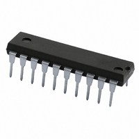
IC CTRL PARALLEL/I2C BUS 20-DIP
Manufacturer
NXP Semiconductors
Datasheet
1.PCF8584P112.pdf
(40 pages)
Specifications of PCF8584P,112
Package / Case
20-DIP (0.300", 7.62mm)
Controller Type
Parallel Bus to I²C Bus Controller
Interface
Parallel
Voltage - Supply
4.5 V ~ 5.5 V
Current - Supply
1.5mA
Operating Temperature
-40°C ~ 85°C
Mounting Type
Through Hole
Maximum Operating Temperature
+ 85 C
Minimum Operating Temperature
- 40 C
Mounting Style
Through Hole
Operating Supply Voltage
4.5 V to 5.5 V
Lead Free Status / RoHS Status
Lead free / RoHS Compliant
Lead Free Status / RoHS Status
Lead free / RoHS Compliant, Lead free / RoHS Compliant
Other names
568-3532-5
935069300112
PCF8584PN
935069300112
PCF8584PN


Philips Semiconductors
6.8.1
The write-only section of S1 enables access to registers S0, S0', S1, S2 and S3, and controls I
Table 4.
6.8.1.1
When the PIN bit is written with a logic 1, all status bits are reset to logic 0. This may serve as a software reset function
(see Figs 5 to 9). PIN is the only bit in S1 which may be both read and written to. PIN is mostly used as a status bit for
synchronizing serial communication, see Section 6.8.2.
6.8.1.2
ESO enables or disables the serial I
ESO is HIGH, I
status bits are made available for reading.
Table 5 Register access control; ESO = 0 (serial interface off) and ESO = 1 (serial interface on)
Notes
1. With ESO = 0, bits ENI, STA, STO and ACK of S1 can be read for test purposes.
2. ‘X’ if ENI = 0.
6.8.1.3
ES1 and ES2 control selection of other registers for initialization and control of normal operation. After these bits are
programmed for access to the desired register (shown in Table 5), the register is selected by a logic LOW level on
register select pin A0.
6.8.1.4
This bit enables the external interrupt output INT, which is generated when the PIN bit is active (logic 0).
This bit must be set to logic 0 before entering the long-distance mode, and remain at logic 0 during operation in
long-distance mode.
1997 Oct 21
ESO = 0; serial interface off (see note 1)
ESO = 1; serial interface on
I
2
C-bus controller
A0
X
1
0
0
0
1
1
0
0
R
EGISTER
PIN (Pending Interrupt Not)
ESO (Enable Serial Output)
ES1 and ES2
ENI
2
C-bus communication is enabled; communication with serial shift register S0 is enabled and the S1 bus
S1
CONTROL SECTION
ES1
0
0
0
1
0
0
0
0
0
INTERNAL REGISTER ADDRESSING 2-WIRE MODE
2
C-bus I/O. When ESO is LOW, register access for initialization is possible. When
ES2
X
X
X
X
0
1
0
0
1
10
IACK
1
1
1
1
0
1
1
1
1
(2)
(2)
(2)
(2)
R/W S1: control
R/W S0': (own address)
R/W S3: (interrupt vector)
R/W S2: (clock register)
W S1: control
R S1; status
R/W S0: (data)
R/W S3: (interrupt vector)
R S3: (interrupt vector ACK cycle))
FUNCTION
2
C-bus operation; see
Product specification
PCF8584
Related parts for PCF8584P,112
Image
Part Number
Description
Manufacturer
Datasheet
Request
R

Part Number:
Description:
Manufacturer:
NXP Semiconductors
Datasheet:

Part Number:
Description:
Manufacturer:
NXP Semiconductors
Datasheet:
Part Number:
Description:
NXP Semiconductors designed the LPC2420/2460 microcontroller around a 16-bit/32-bitARM7TDMI-S CPU core with real-time debug interfaces that include both JTAG andembedded trace
Manufacturer:
NXP Semiconductors
Datasheet:

Part Number:
Description:
NXP Semiconductors designed the LPC2458 microcontroller around a 16-bit/32-bitARM7TDMI-S CPU core with real-time debug interfaces that include both JTAG andembedded trace
Manufacturer:
NXP Semiconductors
Datasheet:
Part Number:
Description:
NXP Semiconductors designed the LPC2468 microcontroller around a 16-bit/32-bitARM7TDMI-S CPU core with real-time debug interfaces that include both JTAG andembedded trace
Manufacturer:
NXP Semiconductors
Datasheet:
Part Number:
Description:
NXP Semiconductors designed the LPC2470 microcontroller, powered by theARM7TDMI-S core, to be a highly integrated microcontroller for a wide range ofapplications that require advanced communications and high quality graphic displays
Manufacturer:
NXP Semiconductors
Datasheet:
Part Number:
Description:
NXP Semiconductors designed the LPC2478 microcontroller, powered by theARM7TDMI-S core, to be a highly integrated microcontroller for a wide range ofapplications that require advanced communications and high quality graphic displays
Manufacturer:
NXP Semiconductors
Datasheet:
Part Number:
Description:
The Philips Semiconductors XA (eXtended Architecture) family of 16-bit single-chip microcontrollers is powerful enough to easily handle the requirements of high performance embedded applications, yet inexpensive enough to compete in the market for hi
Manufacturer:
NXP Semiconductors
Datasheet:
Part Number:
Description:
The XA-S3 device is a member of Philips Semiconductors? XA(eXtended Architecture) family of high performance 16-bitsingle-chip microcontrollers
Manufacturer:
NXP Semiconductors
Datasheet:

Part Number:
Description:
The NXP BlueStreak LH75401/LH75411 family consists of two low-cost 16/32-bit System-on-Chip (SoC) devices
Manufacturer:
NXP Semiconductors
Datasheet:
Part Number:
Description:
The NXP LPC3130/3131 combine an 180 MHz ARM926EJ-S CPU core, high-speed USB2
Manufacturer:
NXP Semiconductors
Datasheet:
Part Number:
Description:
The NXP LPC3141 combine a 270 MHz ARM926EJ-S CPU core, High-speed USB 2
Manufacturer:
NXP Semiconductors
Part Number:
Description:
The NXP LPC3143 combine a 270 MHz ARM926EJ-S CPU core, High-speed USB 2
Manufacturer:
NXP Semiconductors

Part Number:
Description:
The NXP LPC3152 combines an 180 MHz ARM926EJ-S CPU core, High-speed USB 2
Manufacturer:
NXP Semiconductors