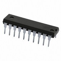
PCF8584P,112 NXP Semiconductors, PCF8584P,112 Datasheet - Page 12

PCF8584P,112
Manufacturer Part Number
PCF8584P,112
Description
IC CTRL PARALLEL/I2C BUS 20-DIP
Manufacturer
NXP Semiconductors
Datasheet
1.PCF8584P112.pdf
(40 pages)
Specifications of PCF8584P,112
Package / Case
20-DIP (0.300", 7.62mm)
Controller Type
Parallel Bus to I²C Bus Controller
Interface
Parallel
Voltage - Supply
4.5 V ~ 5.5 V
Current - Supply
1.5mA
Operating Temperature
-40°C ~ 85°C
Mounting Type
Through Hole
Maximum Operating Temperature
+ 85 C
Minimum Operating Temperature
- 40 C
Mounting Style
Through Hole
Operating Supply Voltage
4.5 V to 5.5 V
Lead Free Status / RoHS Status
Lead free / RoHS Compliant
Lead Free Status / RoHS Status
Lead free / RoHS Compliant, Lead free / RoHS Compliant
Other names
568-3532-5
935069300112
PCF8584PN
935069300112
PCF8584PN
Philips Semiconductors
6.8.2.1
‘Pending Interrupt Not’ (MSB of register S1) is a status flag
which is used to synchronize serial communication and is
set to logic 0 whenever the PCF8584 requires servicing.
The PIN bit is normally read in polled applications to
determine when an I
completed. The PIN bit may also be written, see
Section 6.8.1.
Each time a serial data transmission is initiated (by setting
the STA bit in the same register), the PIN bit will be set to
logic 1 automatically (inactive). When acting as
transmitter, PIN is also set to logic 1 (inactive) each time
S0 is written. In receiver mode, the PIN bit is automatically
set to logic 1 (inactive) each time the data register S0 is
read.
After transmission or reception of one byte on the I
(9 clock pulses, including acknowledge), the PIN bit will be
automatically reset to logic 0 (active) indicating a complete
byte transmission/reception. When the PIN bit is
subsequently set to logic 1 (inactive), all status bits will be
reset to logic 0. PIN is also set to zero on a BER (bus error)
condition.
In polled applications, the PIN bit is tested to determine
when a serial transmission/reception has been completed.
When the ENI bit (bit 4 of write-only section of register S1)
is also set to logic 1 the hardware interrupt is enabled.
In this case, the PIN flag also triggers an external interrupt
(active LOW) via the INT output each time PIN is reset to
logic 0 (active).
When acting as slave transmitter or slave receiver, while
PIN = 0, the PCF8584 will suspend I
by holding the SCL line LOW until the PIN bit is set to
logic 1 (inactive). This prevents further data from being
transmitted or received until the current data byte in S0 has
been read (when acting as slave receiver) or the next data
byte is written to S0 (when acting as slave transmitter).
PIN bit summary:
1997 Oct 21
The PIN bit can be used in polled applications to test
when a serial transmission has been completed. When
the ENI bit is also set, the PIN flag sets the external
interrupt via the INT output.
Setting the STA bit (start bit) will set PIN = 1 (inactive).
In transmitter mode, after successful transmission of
one byte on the I
reset to logic 0 (active) indicating a complete byte
transmission.
In transmitter mode, PIN is set to logic 1 (inactive) each
time register S0 is written.
I
2
C-bus controller
PIN bit
2
C-bus the PIN bit will be automatically
2
C-bus byte transmission/reception is
2
C-bus transmission
2
C-bus
12
6.8.2.2
When in slave receiver mode, this flag is asserted when an
externally generated STOP condition is detected (used
only in slave receiver mode).
6.8.2.3
Bus error; a misplaced START or STOP condition has
been detected. Resets BB (to logic 1; inactive), sets
PIN = 0 (active).
6.8.2.4
‘Last Received Bit’ or ‘Address 0 (General Call) bit’. This
status bit serves a dual function, and is valid only while
PIN = 0:
1. LRB holds the value of the last received bit over the
2. AD0; when AAS = 1 (‘Addressed As Slave’ condition),
6.8.2.5
‘Addressed As Slave’ bit. Valid only when PIN = 0. When
acting as slave receiver, this flag is set when an incoming
address over the I
address register S0' (shifted by one bit, see Section 6.4),
or if the I
received (‘General Call’ is indicated when AD0 status bit is
also set to logic 1, see Section 6.8.2.4).
6.8.2.6
‘Lost Arbitration’ Bit. This bit is set when, in multi-master
operation, arbitration is lost to another master on the
I
2
C-bus.
In receiver mode, PIN is set to logic 0 (active) on
completion of each received byte. Subsequently, the
SCL line will be held LOW until PIN is set to logic 1.
In receiver mode, when register S0 is read, PIN is set to
logic 1 (inactive).
In slave receiver mode, an I
set PIN = 0 (active).
PIN = 0 if a bus error (BER) occurs.
I
Normally this will be the value of the slave
acknowledgement; thus checking for slave
acknowledgement is done via testing of the LRB.
the I
Under this condition, this bit becomes the ‘AD0’ bit and
will be set to logic 1 if the slave address received was
the ‘general call’ (00H) address, or logic 0 if it was the
I
2
2
C-bus while AAS = 0 (not addressed as slave).
C-bus controller’s own slave address.
2
2
C-bus controller has been addressed as a slave.
C-bus ‘General Call’ address (00H) has been
STS
BER
LRB/AD0
AAS
LAB
2
C-bus matches the value in own
2
C-bus STOP condition will
Product specification
PCF8584


