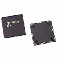
Z16C3510VSG Zilog, Z16C3510VSG Datasheet - Page 166

Z16C3510VSG
Manufacturer Part Number
Z16C3510VSG
Description
IC 10MHZ Z8500 CMOS ISCC 68-PLCC
Manufacturer
Zilog
Series
IUSC™r
Specifications of Z16C3510VSG
Controller Type
Serial Communications Controller (SCC)
Interface
USB
Voltage - Supply
4.75 V ~ 5.25 V
Current - Supply
50mA
Operating Temperature
0°C ~ 70°C
Mounting Type
Surface Mount
Package / Case
68-LCC (J-Lead)
Lead Free Status / RoHS Status
Lead free / RoHS Compliant
Available stocks
Company
Part Number
Manufacturer
Quantity
Price
- Current page: 166 of 268
- Download datasheet (3Mb)
Application Note
The Zilog Datacom Family with the 80186 CPU
SERIAL INTERFACING (Continued)
Note:
[3] Various conventions have been used to combine synchronous clock inputs and modem control inputs on Apple Macintosh connectors
similar to J4, as described in a later section.
Comparison of the two preceding charts leads to several
conclusions:
Finally, an unpopulated 4-pin oscillator socket is included
on the board with its output connected to a single
jumper/wire-wrap pin. This socket can be populated with a
user-supplied oscillator and connected to various clock
pin(s) among J5-J15.
9-12
Pin #
7
8
9
10
11
12
13
14
15
16
Pin #
1
2
3
4
5
6
7
8
9
10
11
12
Pins 1-5 can always be jumpered straight across from a
J5-J10 connector block to a J13-J15 connector block.
In a synchronous environment, the Transmit clock can
be either driven or received and the Receive clock can
be received from the DTE connector or sent on the DCE
connector.
J13-J14
DTE signal
/DCD
GND
/RxC
/TxCO
/TxCI
/RI
Table 10. Pin Assignments of Line Driver/Receiver Connectors
Table 11. Pin Assignments of Controller Port Connectors
J13-J14
DCE signal
/DCD
GND
/RxC
/TxCI
/TxCO
/RI
J11: IUSC Signal
PORT1 (Clock 1 In)
PORT4 (Xmit TSA Gate Out)
(N/C)
PORT0 (Clock 0 In)
(N/C)
PORT3 (Rcv TSA Gate Out)
(N/C)
PORT5 (Rcv Sync Out)
PORT2
GND
PORT6 (Rcv Sync In)
PORT7 (Xmit Complete Out)
J15
DTE signal
/DDC
GND
/RxC
/TxCO
/TxCI
The 10-pin J11 and J12 jumper blocks provide for
connections to the Port pins of the IUSC and (M)USC,
respectively. As with J5-J10, these connections may be to
the customer’s off-board custom circuits and/or to certain
pins in the J13-J15 blocks. The following pin assignment is
determined so that if a 2-channel USC is plugged into the
(M)USC socket, J12 has the same pin-out for the USC’s B
channel as do J5-J10 for other channels.
J15
DCE signal
/DCD
GND
/RxC
/TxCI
/TxCO
J12: (M)USC Signal
PORT1
PORT4 (Xmit TSA Gate Out)
(N/C)
PORT0
(N/C)
PORT3 (Rcv TSA Gate Out)
(SYSCLK)
PORT5 (Rcv Sync Out)
PORT2
GND
PORT6 (Rcv Sync In)
PORT7 (Xmit Complete Out)
Direction/where used
Output to J1B, J2B, J3B
Input from J1A, J2A, J3A, J4
Output to J1B, J2B, J3B
Input from J1A, J2A, J3A
Output to J1-3
Input from J1-3 [3]
Output to J1B, J2B
Input from J1A, J2A
UM011001-0601
Related parts for Z16C3510VSG
Image
Part Number
Description
Manufacturer
Datasheet
Request
R

Part Number:
Description:
CMOS ISCC INTEGRATED SERIAL COMMUNICATIONS CONTROLLER
Manufacturer:
ZILOG [Zilog, Inc.]
Datasheet:

Part Number:
Description:
Communication Controllers, ZILOG INTELLIGENT PERIPHERAL CONTROLLER (ZIP)
Manufacturer:
Zilog, Inc.
Datasheet:

Part Number:
Description:
KIT DEV FOR Z8 ENCORE 16K TO 64K
Manufacturer:
Zilog
Datasheet:

Part Number:
Description:
KIT DEV Z8 ENCORE XP 28-PIN
Manufacturer:
Zilog
Datasheet:

Part Number:
Description:
DEV KIT FOR Z8 ENCORE 8K/4K
Manufacturer:
Zilog
Datasheet:

Part Number:
Description:
KIT DEV Z8 ENCORE XP 28-PIN
Manufacturer:
Zilog
Datasheet:

Part Number:
Description:
DEV KIT FOR Z8 ENCORE 4K TO 8K
Manufacturer:
Zilog
Datasheet:

Part Number:
Description:
CMOS Z8 microcontroller. ROM 16 Kbytes, RAM 256 bytes, speed 16 MHz, 32 lines I/O, 3.0V to 5.5V
Manufacturer:
Zilog, Inc.
Datasheet:

Part Number:
Description:
Low-cost microcontroller. 512 bytes ROM, 61 bytes RAM, 8 MHz
Manufacturer:
Zilog, Inc.
Datasheet:

Part Number:
Description:
Z8 4K OTP Microcontroller
Manufacturer:
Zilog, Inc.
Datasheet:

Part Number:
Description:
CMOS SUPER8 ROMLESS MCU
Manufacturer:
Zilog, Inc.
Datasheet:

Part Number:
Description:
SL1866 CMOSZ8 OTP Microcontroller
Manufacturer:
Zilog, Inc.
Datasheet:

Part Number:
Description:
SL1866 CMOSZ8 OTP Microcontroller
Manufacturer:
Zilog, Inc.
Datasheet:

Part Number:
Description:
OTP (KB) = 1, RAM = 125, Speed = 12, I/O = 14, 8-bit Timers = 2, Comm Interfaces Other Features = Por, LV Protect, Voltage = 4.5-5.5V
Manufacturer:
Zilog, Inc.
Datasheet:


