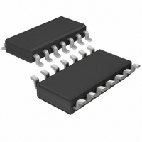
LTC1687IS Linear Technology, LTC1687IS Datasheet - Page 6

LTC1687IS
Manufacturer Part Number
LTC1687IS
Description
IC TXRX RS485 PREC DELAY 14-SOIC
Manufacturer
Linear Technology
Type
Transceiverr
Datasheet
1.LTC1687CSPBF.pdf
(12 pages)
Specifications of LTC1687IS
Number Of Drivers/receivers
1/1
Protocol
RS422, RS485
Voltage - Supply
4.75 V ~ 5.25 V
Mounting Type
Surface Mount
Package / Case
14-SOIC (3.9mm Width), 14-SOL
Lead Free Status / RoHS Status
Contains lead / RoHS non-compliant
Available stocks
Company
Part Number
Manufacturer
Quantity
Price
Company:
Part Number:
LTC1687IS#PBF
Manufacturer:
LTC
Quantity:
1 344
PIN
LTC1686/LTC1687
DE (Pin 4): Driver Enable. DE = high enables the driver.
DE = low will force the driver output into a high impedance
state. Do not float.
D (Pin 5): Driver Input. Controls the states of the Y and Z
outputs when DE = high. Do not float.
GND (Pins 6, 7): Ground.
Y (Pin 9): Noninverting Driver Output.
FU CTIO TABLES
Transmitting
6
TEST CIRCUITS
RE
X
X
X
X
U
U
D
FUNCTIONS
INPUTS
3V
Figure 3. Driver/Receiver Timing Test Circuit
DE
DE
1
1
0
1
U
Y
Z
U
Figure 1. Driver DC Test Load
D
1
0
X
X
Y
U
Z
R
DIFF
V
OD
CONDITION
No Fault
No Fault
LINE
Fault
X
(LTC1687)
C
C
R
R
1686/87 • F01
L1
L2
V
OC
A
B
Hi- Z
Z
0
1
10mA Current
OUTPUTS
Source
RE
15pF
R
Hi- Z
1686/87 F03
Y
1
0
Z (Pin 10): Inverting Driver Output.
B (Pin 11): Inverting Receiver Input.
A (Pin 12): Noninverting Receiver Input.
V
0.1 F ceramic capacitor.
Receiving
DD
RE
0
0
0
0
1
INPUTS
(Pin 14): Positive Supply, 5V to 5%. Bypass with
RECEIVER
UNDER TEST
OUTPUT
OUTPUT
DE
X
X
X
X
X
Figure 4. Driver Timing Test Load #2
TEST POINT
Figure 2. Driver DC Test Load
Inputs Shorted Together
C
15pF
L
C
A = B = – 7V to 12V
500
L
Inputs Open
– 300mV
A – B
300mV
1k
X
S1
S2
S1
S2
1k
1686/87 F04
1686/87 F02
V
OUTPUT
V
DD
DD
Hi- Z
R
1
0
1
1


