CDB1601-120W-Z Cirrus Logic Inc, CDB1601-120W-Z Datasheet - Page 11
CDB1601-120W-Z
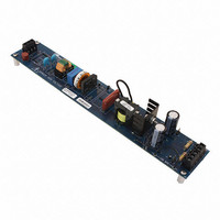
Manufacturer Part Number
CDB1601-120W-Z
Description
High-efficiency PFC Demo. Board
Manufacturer
Cirrus Logic Inc
Series
-r
Datasheets
1.CDB150X-01-Z.pdf
(2 pages)
2.CDB1601-120W-Z.pdf
(24 pages)
3.CDB1601-120W-Z.pdf
(16 pages)
Specifications of CDB1601-120W-Z
Silicon Manufacturer
Cirrus Logic
Kit Application Type
Power Management
Application Sub Type
Power Factor Correction (PFC)
Kit Contents
Board, Datasheet
Design Resources
CS150x/160x PCB Layout Guidelines
Featured Product
CS1501/CS1601 Power Factor Correction IC Controllers
Main Purpose
Power Management, Power Factor Correction
Embedded
No
Utilized Ic / Part
CS1601
Primary Attributes
108 ~ 305 VAC Input, 460V 120W Output
Secondary Attributes
Ballast Control, Up to 2 T5 Lamps
Lead Free Status / Rohs Status
Lead free / RoHS Compliant


5.5 PFC Output Capacitor
The value of the PFC output capacitor should be chosen
based upon voltage ripple and hold-up requirements. To
ensure system stability with the digital controller, the
recommended value of the capacitor is within the range of
0.25F/watt to 0.5F/watt with a V
5.6 Output IFB Sense & Input IAC Sense
A current proportional to the PFC output voltage, V
supplied to the IC on pin IFB and is used as a feedback control
signal. This current is compared against an internal fixed-
value reference current.
The ADC is used to measure the magnitude of the I
through resistor R
compared to an internal reference current of (I
Resistor R
follows:
By using digital loop compensation, the voltage feedback
signal does not require an external compensation network.
A current proportional to the AC input voltage is supplied to the
IC on pin IAC and is used by the PFC control algorithm.
Resistor R
DS931PP6
V
IAC
IFB
I
I
FB
rec t
R
AC
IFB
Figure 19. IAC Input Pin Model
Figure 18. IFB Input Pin Model
sets the IAC current and is derived as follows:
sets the feedback current and is calculated as
IFB
=
. The magnitude of the I
R5
R6
V
---------------------------- -
R1
R2
link
R
R
R
IFB
I
IA C
IAC
ref
IFB
–
IAC
V
1
3
DD
=
R
=
IFB
8
8
link
15 k
V
15 k
460V V
------------------------------ -
V D D
V D D
24 k
24 k
link
129mA
voltage of 460V.
–
IFB
CS1601
CS1601
DD
ref
ADC
ADC
current is then
) 129A.
IFB
current
[Eq.4]
link
[Eq.5]
, is
For optimal performance, resistors R
tolerance or better resistors for best V
5.7 Valley Switching
The zero-current detection (ZCD) pin is monitored for
demagnetization in the auxiliary winding of the boost inductor
(L
valley/zero crossings by sensing the voltage transformed onto
the auxiliary winding of L
The objective of zero-voltage switching is to initiate each
MOSFET switching cycle when its drain-source voltage is at
the lowest possible voltage potential, thus reducing switching
losses. CS1601 uses an auxiliary winding on the PFC boost
inductor to implement zero-voltage switching.
During each switching cycle, when the boost diode current
reaches zero, the boost MOSFET drain-source voltage begins
oscillating at the resonant frequency of the boost inductor and
MOSFET parasitic output capacitance. The ZCD_below_zero
signal transitions from high to low just prior to a local minimum
of the MOSFET drain-source voltage oscillation. The zero-
crossing detect circuit ensures that a ZCD_below_zero pulse
will only be generated when the comparator output is
continuously high for a nominal time period (t
Therefore, any negative edges on the comparator's output
due to spurious glitches will not cause a pulse to be
generated.
Due to the CS1601's variable-frequency control, the MOSFET
switching cycle will not always be initiated at the first resonant
ZCD_below _zero
B
). The ZCD circuit is designed to detect the V
I
V
Aux
+
Aux
-
Figure 20. ZCD Input Pin Model
Figure 21. Zero-voltage Switch
R3
R4
I
Z CD
ZCD
L
B
ZCD
C
p
N:1
B
5
.
CS1601
V
th( Z CD)
Comparator
+
Demag
-
IAC
link
D2
& R
voltage accuracy.
ZCD_below_zero
FE T Drain
IFB
V
ZCB
should use 1%
link
CS1601
) of 200ns.
Zero Crossing
GD ‘ON’
Detection
Aux
11
Related parts for CDB1601-120W-Z
Image
Part Number
Description
Manufacturer
Datasheet
Request
R

Part Number:
Description:
Development Kit
Manufacturer:
Cirrus Logic Inc
Datasheet:
Part Number:
Description:
Development Kit
Manufacturer:
Cirrus Logic Inc
Datasheet:


Part Number:
Description:
High-efficiency PFC + Fluorescent Lamp Driver Reference Design
Manufacturer:
Cirrus Logic Inc
Datasheet:
Part Number:
Description:
Development Kit
Manufacturer:
Cirrus Logic Inc
Datasheet:
Part Number:
Description:
Development Kit
Manufacturer:
Cirrus Logic Inc
Datasheet:

Part Number:
Description:
Development Kit
Manufacturer:
Cirrus Logic Inc
Datasheet:
Part Number:
Description:
Development Kit
Manufacturer:
Cirrus Logic Inc
Datasheet:
Part Number:
Description:
Development Kit
Manufacturer:
Cirrus Logic Inc
Datasheet:
Part Number:
Description:
Development Kit
Manufacturer:
Cirrus Logic Inc
Datasheet:

Part Number:
Description:
EVALUATION BOARD FOR CS8427
Manufacturer:
Cirrus Logic Inc
Datasheet:

Part Number:
Description:
BOARD EVAL FOR CS8416 RCVR
Manufacturer:
Cirrus Logic Inc
Datasheet:

Part Number:
Description:
EVALUATION BOARD FOR CS8420
Manufacturer:
Cirrus Logic Inc
Datasheet:

Part Number:
Description:
KIT DEVELOPMENT EP9315 ARM9
Manufacturer:
Cirrus Logic Inc
Datasheet:

Part Number:
Description:
KIT DEVELOPMENT EP9302 ARM9
Manufacturer:
Cirrus Logic Inc
Datasheet: