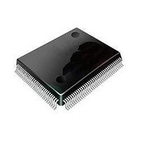
ST92F120V1Q7 STMicroelectronics, ST92F120V1Q7 Datasheet - Page 114

ST92F120V1Q7
Manufacturer Part Number
ST92F120V1Q7
Description
Microcontrollers (MCU) Flash 128K SPI/I2C
Manufacturer
STMicroelectronics
Datasheet
1.ST92F120V9Q7.pdf
(325 pages)
Specifications of ST92F120V1Q7
Data Bus Width
8 bit, 16 bit
Program Memory Type
Flash
Program Memory Size
128 KB
Data Ram Size
4 KB
Interface Type
I2C, SPI
Maximum Clock Frequency
24 MHz
Number Of Programmable I/os
77
Number Of Timers
5
Maximum Operating Temperature
+ 105 C
Mounting Style
SMD/SMT
Package / Case
PQFP-100
Minimum Operating Temperature
- 40 C
On-chip Adc
8 bit, 16 Channel
Lead Free Status / Rohs Status
No
Available stocks
Company
Part Number
Manufacturer
Quantity
Price
Company:
Part Number:
ST92F120V1Q7
Manufacturer:
ST
Quantity:
6 765
Part Number:
ST92F120V1Q7
Manufacturer:
ST
Quantity:
20 000
Part Number:
ST92F120V1Q7C
Manufacturer:
ST
Quantity:
20 000
Company:
Part Number:
ST92F120V1Q7DTR
Manufacturer:
MAXIM
Quantity:
2 854
- Current page: 114 of 325
- Download datasheet (3Mb)
ST92F120 - EXTERNAL MEMORY INTERFACE (EXTMI)
EXTERNAL MEMORY SIGNALS (Cont’d)
Whenever it is sampled low, the System Clock is
stretched and the external memory signals (AS,
DS, DS2, RW, P0 and P1) are released in high-im-
pedance. The external memory interface pins are
driven again by the ST9 as soon as BREQ is sam-
pled high.
BACK (Alternate Function Output, Active low) indi-
cates that the ST9 has relinquished control of the
memory bus in response to a bus request. BREQ
is driven low when the external memory interface
signals are released in high-impedance.
At MCU reset, the bus request function is disabled.
To enable it, configure the I/O port pins assigned
to BREQ and BACK as Alternate Function and set
the BRQEN bit in the MODER register.
8.2.6 PORT 0
If Port 0 (Input/Output, Push-Pull/Open-Drain/
Weak Pull-up) is used as a bit programmable par-
allel I/O port, it has the same features as a regular
port. When set as an Alternate Function, it is used
as the External Memory interface: it outputs the
multiplexed Address 8 LSB: A[7:0] /Data bus
D[7:0].
8.2.7 PORT 1
If Port 1 (Input/Output, Push-Pull/Open-Drain/
Weak Pull-up) is used as a bit programmable par-
allel I/O port, it has the same features as a regular
port. When set as an Alternate Function, it is used
Figure 60. Application Example
114/324
9
ST9+
RW
P0
AS
DS
P1
A15-A8
A0-A7/D0-D7
D1-D8
OE
LE
LATCH
Q1-Q8
as the external memory interface to provide the 8
MSB of the address A[15:8].
The behavior of the Port 0 and 1 pins is affected by
the BSZ and ETO bits in the EMR1 register. Refer
to the Register description.
8.2.8 WAIT: External Memory Wait
WAIT (Alternate Function Input, Active low) indi-
cates to the ST9 that the external memory requires
more time to complete the memory access cycle. If
bit EWEN (EIVR) is set, the WAIT signal is sam-
pled with the rising edge of the processor internal
clock during phase T1 or T2 of every memory cy-
cle. If the signal was sampled active, one more in-
ternal clock cycle is added to the memory cycle.
On the rising edge of the added internal clock cy-
cle, WAIT is sampled again to continue or finish
the memory cycle stretching. Note that if WAIT is
sampled active during phase T1 then AS is
stretched, while if WAIT is sampled active during
phase T2 then DS is stretched. WAIT is enabled
via software as the Alternate Function input of the
associated I/O port bit (refer to specific ST9 ver-
sion to identify the specific port and pin). Under
Reset status, the associated bit of the port is set to
the bidirectional weak pull-up mode. Refer to
ure
59.
Q0-Q7
A0-A15
E
G
W
64 Kbytes
RAM
Fig-
Related parts for ST92F120V1Q7
Image
Part Number
Description
Manufacturer
Datasheet
Request
R

Part Number:
Description:
8/16-bit Flash Mcu Family With Ram, Eeprom And J1850 Blpd
Manufacturer:
STMicroelectronics
Datasheet:

Part Number:
Description:
STMicroelectronics [RIPPLE-CARRY BINARY COUNTER/DIVIDERS]
Manufacturer:
STMicroelectronics
Datasheet:

Part Number:
Description:
STMicroelectronics [LIQUID-CRYSTAL DISPLAY DRIVERS]
Manufacturer:
STMicroelectronics
Datasheet:

Part Number:
Description:
BOARD EVAL FOR MEMS SENSORS
Manufacturer:
STMicroelectronics
Datasheet:

Part Number:
Description:
NPN TRANSISTOR POWER MODULE
Manufacturer:
STMicroelectronics
Datasheet:

Part Number:
Description:
TURBOSWITCH ULTRA-FAST HIGH VOLTAGE DIODE
Manufacturer:
STMicroelectronics
Datasheet:

Part Number:
Description:
Manufacturer:
STMicroelectronics
Datasheet:

Part Number:
Description:
DIODE / SCR MODULE
Manufacturer:
STMicroelectronics
Datasheet:

Part Number:
Description:
DIODE / SCR MODULE
Manufacturer:
STMicroelectronics
Datasheet:

Part Number:
Description:
Search -----> STE16N100
Manufacturer:
STMicroelectronics
Datasheet:

Part Number:
Description:
Search ---> STE53NA50
Manufacturer:
STMicroelectronics
Datasheet:

Part Number:
Description:
NPN Transistor Power Module
Manufacturer:
STMicroelectronics
Datasheet:


