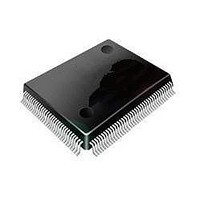
ST92F120V1Q7 STMicroelectronics, ST92F120V1Q7 Datasheet - Page 122

ST92F120V1Q7
Manufacturer Part Number
ST92F120V1Q7
Description
Microcontrollers (MCU) Flash 128K SPI/I2C
Manufacturer
STMicroelectronics
Datasheet
1.ST92F120V9Q7.pdf
(325 pages)
Specifications of ST92F120V1Q7
Data Bus Width
8 bit, 16 bit
Program Memory Type
Flash
Program Memory Size
128 KB
Data Ram Size
4 KB
Interface Type
I2C, SPI
Maximum Clock Frequency
24 MHz
Number Of Programmable I/os
77
Number Of Timers
5
Maximum Operating Temperature
+ 105 C
Mounting Style
SMD/SMT
Package / Case
PQFP-100
Minimum Operating Temperature
- 40 C
On-chip Adc
8 bit, 16 Channel
Lead Free Status / Rohs Status
No
Available stocks
Company
Part Number
Manufacturer
Quantity
Price
Company:
Part Number:
ST92F120V1Q7
Manufacturer:
ST
Quantity:
6 765
Part Number:
ST92F120V1Q7
Manufacturer:
ST
Quantity:
20 000
Part Number:
ST92F120V1Q7C
Manufacturer:
ST
Quantity:
20 000
Company:
Part Number:
ST92F120V1Q7DTR
Manufacturer:
MAXIM
Quantity:
2 854
- Current page: 122 of 325
- Download datasheet (3Mb)
ST92F120 - I/O PORTS
INPUT/OUTPUT BIT CONFIGURATION (Cont’d)
When Px.n is programmed as an Output:
(Figure
– The Output Buffer is turned on in an Open-drain
– The data stored in the Output Master Latch is
When Px.n is programmed as Bidirectional:
(Figure
– The Output Buffer is turned on in an Open-Drain
– The data present on the I/O pin is sampled into
– The data stored in the Output Master Latch is
WARNING: Due to the fact that in bidirectional
mode the external pin is read instead of the output
latch, particular care must be taken with arithme-
tic/logic and Boolean instructions performed on a
bidirectional port pin.
These instructions use a read-modify-write se-
quence, and the result written in the port register
depends on the logical level present on the exter-
nal pin.
This may bring unwanted modifications to the port
output register content.
For example:
Port register content, 0Fh
external port value, 03h
(Bits 3 and 2 are externally forced to 0)
A bset instruction on bit 7 will return:
Port register content, 83h
external port value, 83h
(Bits 3 and 2 have been cleared).
To avoid this situation, it is suggested that all oper-
ations on a port, using at least one bit in bidirec-
tional mode, are performed on a copy of the port
register, then transferring the result with a load in-
struction to the I/O port.
When Px.n is programmed as a digital Alter-
nate Function Output:
(Figure
– The Output Buffer is turned on in an Open-Drain
122/324
9
or Push-pull configuration.
copied both into the Input Latch and into the Out-
put Slave Latch, driving the I/O pin, at the end of
the execution of the instruction.
or Weak Pull-up configuration (except when dis-
abled in hardware).
the Input Latch at the beginning of the execution
of the instruction.
copied into the Output Slave Latch, driving the I/
O pin, at the end of the execution of the instruc-
tion.
or Push-Pull configuration.
5)
6)
7)
– The data present on the I/O pin is sampled into
– The signal from an on-chip function is allowed to
Figure 66. Bidirectional Configuration
n
n
Figure 67. Alternate Function Configuration
n
n
n
n
n
n
the Input Latch at the beginning of the execution
of the instruction.
load the Output Slave Latch driving the I/O pin.
Signal timing is under control of the alternate
function. If no alternate function is connected to
Px.n, the I/O pin is driven to a high level when in
Push-Pull configuration, and to a high imped-
ance state when in open drain configuration.
WEAK PULL-UP
OPEN DRAIN
OPEN DRAIN
PUSH-PULL
PERIPHERAL
OUTPUT MASTER LATCH
OUTPUT SLAVE LATCH
OUTPUT
OUTPUT SLAVE LATCH
FROM
INTERNAL DATA BUS
INTERNAL DATA BUS
I/O PIN
I/O PIN
INPUT LATCH
INPUT LATCH
(or Schmitt Trigger)
(or Schmitt Trigger)
TO PERIPHERAL
INTERRUPTS
INPUTS AND
TO PERIPHERAL
INTERRUPTS
INPUTS AND
TTL
TTL
Related parts for ST92F120V1Q7
Image
Part Number
Description
Manufacturer
Datasheet
Request
R

Part Number:
Description:
8/16-bit Flash Mcu Family With Ram, Eeprom And J1850 Blpd
Manufacturer:
STMicroelectronics
Datasheet:

Part Number:
Description:
STMicroelectronics [RIPPLE-CARRY BINARY COUNTER/DIVIDERS]
Manufacturer:
STMicroelectronics
Datasheet:

Part Number:
Description:
STMicroelectronics [LIQUID-CRYSTAL DISPLAY DRIVERS]
Manufacturer:
STMicroelectronics
Datasheet:

Part Number:
Description:
BOARD EVAL FOR MEMS SENSORS
Manufacturer:
STMicroelectronics
Datasheet:

Part Number:
Description:
NPN TRANSISTOR POWER MODULE
Manufacturer:
STMicroelectronics
Datasheet:

Part Number:
Description:
TURBOSWITCH ULTRA-FAST HIGH VOLTAGE DIODE
Manufacturer:
STMicroelectronics
Datasheet:

Part Number:
Description:
Manufacturer:
STMicroelectronics
Datasheet:

Part Number:
Description:
DIODE / SCR MODULE
Manufacturer:
STMicroelectronics
Datasheet:

Part Number:
Description:
DIODE / SCR MODULE
Manufacturer:
STMicroelectronics
Datasheet:

Part Number:
Description:
Search -----> STE16N100
Manufacturer:
STMicroelectronics
Datasheet:

Part Number:
Description:
Search ---> STE53NA50
Manufacturer:
STMicroelectronics
Datasheet:

Part Number:
Description:
NPN Transistor Power Module
Manufacturer:
STMicroelectronics
Datasheet:


