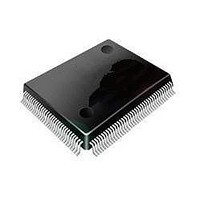
ST92F120V1Q7 STMicroelectronics, ST92F120V1Q7 Datasheet - Page 289

ST92F120V1Q7
Manufacturer Part Number
ST92F120V1Q7
Description
Microcontrollers (MCU) Flash 128K SPI/I2C
Manufacturer
STMicroelectronics
Datasheet
1.ST92F120V9Q7.pdf
(325 pages)
Specifications of ST92F120V1Q7
Data Bus Width
8 bit, 16 bit
Program Memory Type
Flash
Program Memory Size
128 KB
Data Ram Size
4 KB
Interface Type
I2C, SPI
Maximum Clock Frequency
24 MHz
Number Of Programmable I/os
77
Number Of Timers
5
Maximum Operating Temperature
+ 105 C
Mounting Style
SMD/SMT
Package / Case
PQFP-100
Minimum Operating Temperature
- 40 C
On-chip Adc
8 bit, 16 Channel
Lead Free Status / Rohs Status
No
Available stocks
Company
Part Number
Manufacturer
Quantity
Price
Company:
Part Number:
ST92F120V1Q7
Manufacturer:
ST
Quantity:
6 765
Part Number:
ST92F120V1Q7
Manufacturer:
ST
Quantity:
20 000
Part Number:
ST92F120V1Q7C
Manufacturer:
ST
Quantity:
20 000
Company:
Part Number:
ST92F120V1Q7DTR
Manufacturer:
MAXIM
Quantity:
2 854
- Current page: 289 of 325
- Download datasheet (3Mb)
Note:
(2) Hysteresis voltage between switching levels: characterization results - not tested.
(3) For a description of the EMR1 Register - BSZ bit refer to the External Memory Interface Chapter.
(4) Not 100% tested, guaranteed by design characterisation. The absolute sum of input overload currents on all port pins may no t exceed
(5) Indicative values extracted from Design simulation.
(1) Unless otherwise stated, typical data are based on T
Symbol
R
I
I
V
I
LKIOD
LKA/D
V
SR
SR
V
LKIO
I
100 mA.
WPU
production. Hysteresis voltage between switching levels: characterization results - not tested.
HYS
OV
OH
OL
R
F
Input Hysteresis
Standard Schmitt Trigger
P2[5:4]-P2[1:0]-P3[7:4] P3[2:1]-
P4[4:3]-P4[1:0] P5[7:4]-P5[2:0]-
P6[3:0] P7[7:0]-P8[7:0]-P9[7:0]
Input Hysteresis
Special Schmitt Trigger
P4[7:6]
Input Hysteresis
High Hyst. Schmitt Trigger
P6[5:4]
Output High Level
P0[7:0]-P6[5:4]
AS-DS-RW
Output High Level
P1[7:0]-P2[7:4]-P2[1:0] P3[7:1]-
P4[5:0]-P5[7:0]-P6[3:0]-P7[7:0]-
P8[7:0] P9[7:0]-VPWO
Output Low Level
P0[7:0]-P2[3:2]-P4[7:6] P6[5:4]-
AS-DS-RW
Output Low Level
P1[7:0]-P2[7:4]-P2[1:0] P3[7:1]-
P4[5:0]-P5[7:0]
P6[3:0]-P7[7:0]-P8[7:0] P9[7:0]-
VPWO
Weak Pull-up Current
P2[7:4]-P2[1:0]-P3[7:1]
P4.5-P4[3:1]-P5.3-P6[3:0]
P7[7:0] P8[7:0]-P9[7:0]
Weak Pull-up Current
P6[5:4]-AS-DS
I/O Pin Input Leakage
I/O Pin Open Drain Input Leakage
Overload Current
Slew Rate Rise
Slew Rate Fall
A/D Conv. Input Leakage
Parameter
(2)
(2)
(2)
Push Pull, I
EMR1 Register - BSZ bit = 0
Push Pull, I
EMR1 Register - BSZ bit = 1
Push Pull, I
EMR1 Register - BSZ bit = 0
Push Pull, I
EMR1 Register - BSZ bit = 1
Push Pull / Open Drain, I
EMR1 Register - BSZ bit = 0
Push Pull / Open Drain, I
EMR1 Register - BSZ bit = 1
Push Pull / Open Drain, I
EMR1 Register - BSZ bit = 0
Push Pull / Open Drain, I
EMR1 Register - BSZ bit = 1
Bidirectional Weak Pull-up
V
Bidirectional Weak Pull-up
V
Input/Tri-State,
0V < V
Input/Tri-State,
0V < V
(4)
(5)
(5)
OL
OL
A
= 25°C and V
= 0V
= 0V
IN
IN
ST92F120 - ELECTRICAL CHARACTERISTICS
< V
< V
Comment
OH
OH
OH
OH
DD
DD
= – 2mA
= – 8mA
= – 2mA
= – 4mA
DD
= 5V. They are only reported for design guide lines not tested in
OL
OL
OL
OL
=8mA,
=2mA,
=4mA,
=2mA
(3)
(3)
(3)
(3)
(3)
(3)
(3)
(3)
V
V
V
V
DD
DD
DD
DD
Min
100
– 1
– 1
– 1
30
– 0.8
– 0.8
– 0.8
– 0.8
Typ
Value
600
800
900
100
200
(1)
Max
400
450
0.4
0.4
0.4
0.4
+ 1
+ 1
+ 1
70
70
5
289/324
mA/ns
mA/ns
Unit
mV
mV
mV
mA
V
V
V
V
V
V
V
V
A
A
A
A
A
1
Related parts for ST92F120V1Q7
Image
Part Number
Description
Manufacturer
Datasheet
Request
R

Part Number:
Description:
8/16-bit Flash Mcu Family With Ram, Eeprom And J1850 Blpd
Manufacturer:
STMicroelectronics
Datasheet:

Part Number:
Description:
STMicroelectronics [RIPPLE-CARRY BINARY COUNTER/DIVIDERS]
Manufacturer:
STMicroelectronics
Datasheet:

Part Number:
Description:
STMicroelectronics [LIQUID-CRYSTAL DISPLAY DRIVERS]
Manufacturer:
STMicroelectronics
Datasheet:

Part Number:
Description:
BOARD EVAL FOR MEMS SENSORS
Manufacturer:
STMicroelectronics
Datasheet:

Part Number:
Description:
NPN TRANSISTOR POWER MODULE
Manufacturer:
STMicroelectronics
Datasheet:

Part Number:
Description:
TURBOSWITCH ULTRA-FAST HIGH VOLTAGE DIODE
Manufacturer:
STMicroelectronics
Datasheet:

Part Number:
Description:
Manufacturer:
STMicroelectronics
Datasheet:

Part Number:
Description:
DIODE / SCR MODULE
Manufacturer:
STMicroelectronics
Datasheet:

Part Number:
Description:
DIODE / SCR MODULE
Manufacturer:
STMicroelectronics
Datasheet:

Part Number:
Description:
Search -----> STE16N100
Manufacturer:
STMicroelectronics
Datasheet:

Part Number:
Description:
Search ---> STE53NA50
Manufacturer:
STMicroelectronics
Datasheet:

Part Number:
Description:
NPN Transistor Power Module
Manufacturer:
STMicroelectronics
Datasheet:


