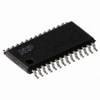
PCA9558PW,118 NXP Semiconductors, PCA9558PW,118 Datasheet - Page 8

PCA9558PW,118
Manufacturer Part Number
PCA9558PW,118
Description
IC I2C SMBUS 8BIT I/O 28TSSOP
Manufacturer
NXP Semiconductors
Datasheet
1.PCA9558PW112.pdf
(27 pages)
Specifications of PCA9558PW,118
Package / Case
28-TSSOP
Applications
PC's, PDA's
Interface
I²C
Voltage - Supply
3 V ~ 3.6 V
Mounting Type
Surface Mount
Logic Family
PCA9558
Number Of Lines (input / Output)
8.0 / 8.0
Propagation Delay Time
21 ns
Operating Supply Voltage
3 V to 3.6 V
Operating Temperature Range
0 C to + 70 C
Input Voltage
5 V
Logic Type
I2C, SMBus
Maximum Clock Frequency
400 KHz
Mounting Style
SMD/SMT
Number Of Input Lines
8.0
Number Of Output Lines
8.0
Output Voltage
5 V
Lead Free Status / RoHS Status
Lead free / RoHS Compliant
Lead Free Status / RoHS Status
Lead free / RoHS Compliant, Lead free / RoHS Compliant
Other names
935269433118
PCA9558PW-T
PCA9558PW-T
PCA9558PW-T
PCA9558PW-T
NXP Semiconductors
PCA9558_4
Product data sheet
Fig 7.
Fig 8.
I
I
2
2
C-bus write for MUXCNTRL register
C-bus read for MUXCNTRL register
S
START condition
S
START condition
7.1.2.1 IP - Input Port register
1
7.1.2 Registers
1
0
0
slave address
slave address
0
0
The GPIOs are controlled by a set of 4 internal registers: Input Port (IP) register; Output
Port (OP) register; Polarity Inversion (PI) register; and the Input/Output Configuration
(IOC) register. Each register is read/write via the I
exception of the Input Port register, which is read only, one at a time. The read/write takes
place on the slave Acknowledge. The control of which register is currently available to the
I
for details.
This register is an input-only port. It reflects the logic value present on the GPIO pins
regardless of whether they are configured as inputs or outputs (IOC register). Writes to
this register have no effect.
Table 5.
1
Bit
Symbol
Default
2
C-bus is set by bits in the control register. See
1
1
1
1 A0 0
1 A0 0
R/W
IP - Input Port register description
R/W
I7
7
0
A
acknowledge
from slave
A
acknowledge
from slave
0
0
0
0
command byte
Rev. 04 — 14 April 2009
0
I6
6
0
command byte
0
0
0
1
1
0
acknowledge
0
acknowledge
I5
5
0
from slave
1
from slave
1
1
1
(cont.)
A
A
S
I4
(re)START
condition
4
0
0
1
0
0
Section 7.1.2.1
0
0
2
C-bus or 256-byte EEPROM, with the
0
slave address
data from slave
0
0
data byte
I3
0
3
0
1
0
0
1
0
8-bit I
no acknowledge
0 B1
acknowledge
1 A0 1
0 B1 B0
from slave
from master
I2
2
0
through
B0
R/W
2
C-bus/SMBus I/O port
A
NA
A
PCA9558
acknowledge
from slave
002aad371
© NXP B.V. 2009. All rights reserved.
P
STOP
condition
002aad372
(cont.)
Section 7.1.2.4
P
STOP
condition
I1
1
0
I0
0
0
8 of 27


