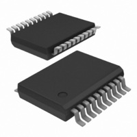
74HC4351DB,112 NXP Semiconductors, 74HC4351DB,112 Datasheet - Page 12

74HC4351DB,112
Manufacturer Part Number
74HC4351DB,112
Description
IC MUX/DEMUX 8X1 20SSOP
Manufacturer
NXP Semiconductors
Series
74HCr
Datasheets
1.74HCT4046ADB112.pdf
(19 pages)
2.74HCT4046ADB112.pdf
(23 pages)
3.74HCT4351D112.pdf
(17 pages)
Specifications of 74HC4351DB,112
Package / Case
20-SSOP (0.200", 5.30mm Width)
Function
Multiplexer/Demultiplexer
Circuit
1 x 8:1
On-state Resistance
60 Ohm
Voltage Supply Source
Dual Supply
Voltage - Supply, Single/dual (±)
±2 V ~ 10 V
Current - Supply
16µA
Mounting Type
Surface Mount
Number Of Channels
1 Channel
On Resistance (max)
180 Ohm @ 4.5 V
Propagation Delay Time
90 ns
On Time (max)
300 ns @ 2 V
Off Time (max)
275 ns @ 2 V
Supply Voltage (max)
10 V
Supply Voltage (min)
2 V
Supply Current
50 mA
Maximum Power Dissipation
500 mW
Maximum Operating Temperature
+ 125 C
Minimum Operating Temperature
- 40 C
Mounting Style
SMD/SMT
Number Of Switches
Single
Off State Leakage Current (max)
1 uA
Switch Current (typ)
25 mA
Lead Free Status / RoHS Status
Lead free / RoHS Compliant
Lead Free Status / RoHS Status
Lead free / RoHS Compliant, Lead free / RoHS Compliant
Other names
568-2702-5
935190070112
935190070112
Philips Semiconductors
Test circuit for 74HC
HCT TYPES
AC waveforms 74HCT
March 1988
handbook, full pagewidth
HCMOS family characteristics
Switch position
Note
1. For open-drain N-channel outputs t
TEST
t
t
t
t
C
R
PZH
PZL
PHZ
PLZ
L
T
=
=
Fig.8 Input rise and fall times, transition times and propagation delays for combinatorial logic ICs.
load capacitance including jig and probe capacitance
(see AC CHARACTERISTICS for values).
termination resistance should be equal to the output impedance Z
the pulse generator.
SWITCH
GND
V
GND
V
CC
CC
handbook, halfpage
GENERATOR
PULSE
INPUT
OUTPUT
Fig.7 Test circuit for 3-state outputs.
PLZ
and t
V I
t PHL
t THL
10%
90%
PZL
R T
t r
1.3 V
are applicable.
90%
1.3 V
10%
D.U.T
V CC
12
o
of
t f
V O
C L
t PLH
t TLH
R L = 1 k
50 pF
MGK567
FAMILY SPECIFICATIONS
3 V
GND
MGK563
V CC


