IDT74GTLP16612PA IDT, Integrated Device Technology Inc, IDT74GTLP16612PA Datasheet - Page 2
IDT74GTLP16612PA
Manufacturer Part Number
IDT74GTLP16612PA
Description
Manufacturer
IDT, Integrated Device Technology Inc
Datasheet
1.IDT74GTLP16612PA.pdf
(8 pages)
Specifications of IDT74GTLP16612PA
Logic Family
GTLP
Operating Supply Voltage (typ)
3.3/5V
Propagation Delay Time
8.7ns
Number Of Elements
1
Number Of Channels
18
Input Logic Level
LVTTL/TTL
Output Logic Level
GTLP
Output Type
3-State/Open Drain
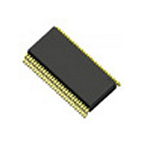
Package Type
TSSOP
Polarity
Non-Inverting
Logical Function
Universal Bus Transceiver with Voltage Translation
Operating Supply Voltage (min)
3.135/4.75V
Operating Supply Voltage (max)
5.25V
Quiescent Current (typ)
30mA
Technology
CMOS
Operating Temp Range
-40C to 85C
Operating Temperature Classification
Industrial
Mounting
Surface Mount
Pin Count
56
Lead Free Status / Rohs Status
Not Compliant


PIN CONFIGURATION
IDT74GTLP16612
CMOS 18-BIT TTL/GTLP UNIVERSAL BUS TRANSCEIVER
V
V
CC
CC
GND
OEBA
LEAB
(3.3V)
LEBA
OEAB
(3.3V)
GND
GND
GND
A
A
A
A
A
A
A
A
A
A
A
A
A
A
A
A
A
A
10
11
12
13
14
15
16
17
18
Q
1
2
3
4
5
6
7
8
9
1
2
3
4
5
6
7
8
9
10
11
12
13
14
15
16
17
18
19
20
21
22
23
24
25
26
27
28
SSOP/ TSSOP
TOP VIEW
56
55
54
53
52
51
50
49
48
47
46
45
44
43
42
41
40
39
38
37
36
35
34
33
32
31
30
29
CEAB
CLKAB
GND
B
B
B
B
B
GND
B
B
B
B
B
B
GND
B
B
B
V
B
B
GND
B
CLKBA
CEBA
V
B
2
3
4
5
6
7
8
9
10
11
12
13
14
15
REF
16
17
18
CCQ
1
(5V)
2
ABSOLUTE MAXIMUM RATINGS
NOTES:
1. Stresses greater than those listed under ABSOLUTE MAXIMUM RATINGS may cause
2. Unused inputs without Bus-Hold must be held HIGH or LOW.
CAPACITANCE (T
NOTES:
1. As applicable to the device type.
2. All typical values are at V
PIN DESCRIPTION
NOTE:
1. A-Port pins have Bus-Hold. All other pins are standard input, output, or I/O.
Symbol
Symbol
permanent damage to the device. This is a stress rating only and functional operation
of the device at these or any other conditions above those indicated in the operational
sections of this specification is not implied. Exposure to absolute maximum rating
conditions for extended periods may affect reliability.
Pin Names
C
C
V
C
T
V
I
V
V
I
I
I
I
A
B
I
I
CLKAB
CLKBA
CCQ
V
I
OL
OH
OL
OK
OK
STG
IN
/
/
OEAB
OEBA
CC
IK
CEAB
CEBA
LEAB
LEBA
O
O
O
O
1
1
V
I
REF
- A
- B
18
18
Control Pins
A-Port
B-Port
Rating
Supply Voltage
DC Input Voltage
DC Output Voltage, 3-State
DC Output Voltage, Active
DC Output Sink Current into A-port
DC Output Source Current from A-port
DC Output Sink Current into B-port
(in the LOW state)
DC Input Diode Current V
DC Output Diode Current V
DC Output Diode Current V
Storage Temperature
Parameter
A-to-B Output Enable (Active LOW)
B-to-A Output Enable (Active LOW)
A-to-B Clock Enable (Active LOW)
B-to-A Clock Enable (Active LOW)
A-to-B Latch Enable (Transparent HIGH)
B-to-A Latch Enable (Transparent HIGH)
A-to-B Clock Pulse
B-to-A Clock Pulse
GTLP Input Reference Voltage
A-to-B TTL Data Inputs or B-to-A 3-State Outputs
B-to-A GTLP Data Inputs or A-to-B Open Drain Outputs
(1)
CC
= 3.3V and V
INDUSTRIAL TEMPERATURE RANGE
V
V
V
A
I
I
I
Conditions
= +25°C, f = 1.0MH
= V
= V
= V
Description
CCQ
CCQ
CCQ
I
< 0V
CCQ
O
O
< 0V
> V
or 0
or 0
or 0
= 5V.
CC
(1)
Typ.
–0.5 to V
8
9
6
–65 to +150
–0.5 to +7
–0.5 to +7
–0.5 to +7
(2)
Max.
+50
–64
–50
–50
64
80
CC
Z
Max.
+ 0.5
)
(1,2)
—
—
—
Unit
Unit
pF
pF
pF
mA
mA
mA
mA
mA
mA
° C
V
V
V
V
Related parts for IDT74GTLP16612PA
Image
Part Number
Description
Manufacturer
Datasheet
Request
R

Part Number:
Description:
TRANSLATION DEVICE DPI 80-PQFP
Manufacturer:
IDT, Integrated Device Technology Inc
Datasheet:
Part Number:
Description:
IDT PART
Manufacturer:
IDT, Integrated Device Technology Inc
Datasheet:
Part Number:
Description:
IC LIU T1/E1/J1 OCTAL 256PBGA
Manufacturer:
IDT, Integrated Device Technology Inc
Datasheet:

Part Number:
Description:
IC FREQ TIMING GENERATOR 28TSSOP
Manufacturer:
IDT, Integrated Device Technology Inc
Datasheet:
Part Number:
Description:
IC CLK DVR PLL 1:10 40VFQFPN
Manufacturer:
IDT, Integrated Device Technology Inc
Datasheet:
Part Number:
Description:
IC CLK FANOUT BUFFER 1:18 32LQFP
Manufacturer:
IDT, Integrated Device Technology Inc
Datasheet:
Part Number:
Description:
IC CLK FANOUT BUFFER 1:18 32LQFP
Manufacturer:
IDT, Integrated Device Technology Inc
Datasheet:
Part Number:
Description:
IC CK505 VREG/RES 56TSSOP
Manufacturer:
IDT, Integrated Device Technology Inc
Datasheet:

Part Number:
Description:
IC SDRAM CLK DVR 1:10 48-TSSOP
Manufacturer:
IDT, Integrated Device Technology Inc
Datasheet:

Part Number:
Description:
IC CLK DVR PLL 1:10 48TSSOP
Manufacturer:
IDT, Integrated Device Technology Inc
Datasheet:
Part Number:
Description:
IC FLEXPC CLK PROGR P4 56-TSSOP
Manufacturer:
IDT, Integrated Device Technology Inc
Datasheet:
Part Number:
Description:
IC FLEXPC CLK PROGR P4 56-TSSOP
Manufacturer:
IDT, Integrated Device Technology Inc
Datasheet:
Part Number:
Description:
IC FLEXPC CLK PROGR P4 56-SSOP
Manufacturer:
IDT, Integrated Device Technology Inc
Datasheet:

Part Number:
Description:
IC PLL CLK DRIVER 2.5V 28-TSSOP
Manufacturer:
IDT, Integrated Device Technology Inc
Datasheet:
Part Number:
Description:
IC CLOCK DRIVER 2.5V 24-TSSOP
Manufacturer:
IDT, Integrated Device Technology Inc
Datasheet: