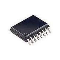
74LV4052PW NXP Semiconductors, 74LV4052PW Datasheet - Page 9

74LV4052PW
Manufacturer Part Number
74LV4052PW
Description
Multiplexer Switch ICs DUAL 4-CH MUX/DMUX
Manufacturer
NXP Semiconductors
Datasheet
1.74LV4052PW118.pdf
(16 pages)
Specifications of 74LV4052PW
Number Of Channels
2 Channel
On Resistance (max)
250 Ohms
Propagation Delay Time
25 ns, 9 ns, 6 ns, 5 ns, 4 ns, 3 ns
On Time (max)
190 ns
Off Time (max)
125 ns
Supply Voltage (max)
6 V
Supply Voltage (min)
1 V
Maximum Power Dissipation
400 mW
Maximum Operating Temperature
+ 125 C
Minimum Operating Temperature
- 40 C
Package / Case
TSSOP-16
Mounting Style
SMD/SMT
Number Of Lines (input / Output)
8 / 2
Lead Free Status / Rohs Status
Details
Other names
74LV4052PW,112
Available stocks
Company
Part Number
Manufacturer
Quantity
Price
Part Number:
74LV4052PW
Manufacturer:
NXP/恩智浦
Quantity:
20 000
Company:
Part Number:
74LV4052PW,118
Manufacturer:
NXP
Quantity:
150
Company:
Part Number:
74LV4052PWЈ¬118
Manufacturer:
NXP
Quantity:
7 500
Test conditions: V
Philips Semiconductors
NOTES TO FIGURES 6 AND 7:
1998 Jun 23
ADDITIONAL AC CHARACTERISTICS
Recommended conditions and typical values
GND = 0 V; t
GENERAL NOTES:
NOTES:
1. V
2. V
1. Adjust input voltage V
2. Adjust input voltage V
SYMBOL
Dual 4-channel analog multiplexer/demultiplexer
V
–100
f
Figure 6. Typical switch “OFF” signal feed-through as a
(dB)
V
(p–p)
max
C
–50
is
OS
is
S
0
is the input voltage at nY or nZ terminal, whichever is assigned as an input.
10
is the output voltage at nY or nZ terminal, whichever is assigned as an output.
0.1 mF
r
= t
Sine-wave distortion
f = 1 kHz
Sine-wave distortion
f = 10 kHz
Switch “OFF” signal feed through
Crosstalk between any two
switches/multiplexers
Crosstalk voltage between enable or
address input to any switch
(peak-to-peak value)
Minimum frequency response
(–3 dB)
Maximum switch capacitance
f
CC
10
2.5ns
R
= 3.0 V; GND = 0 V; V
2
L
function of frequency.
nY
is
is
PARAMETER
n
is 0 dBm level (0 dBm = 1 mW into 600 W).
is 0 dBm level at V
/nZ
10
3
Figure 8. Test circuit for measuring crosstalk between any two switches.
channel
ON
(a)
10
EE
V
(a) channel ON condition; (b) channel OFF condition.
4
CC
f (kHz)
= -3.0 V; R
2R
OS
L
2R
for 1 MHz (0 dBm = 1 mW into 50 W).
L
10
5
L
C
TYP.
0.80
0.40
2.40
1.20
nZ/nY
–50
–50
–60
–60
120
180
200
110
L
SV01635
= 50 W; R
5
n
10
UNIT
MHz
6
mV
dB
dB
GND
%
%
pf
SOURCE
9
V
3.0
6.0
3.0
6.0
3.0
6.0
3.0
6.0
3.0
6.0
3.0
6.0
(V)
CC
nY
= 1kW.
(dB)
n
/nZ
5
0
–5
10
V
Note 1
Note 1
Note 2
is(p–p)
2.75
5.50
2.75
5.50
(V)
2R
R
L
L
V
Figure 7. Typical frequency response.
CC
R
Figure 9 and 10
R
Figure 9 and 10
R
Figures 5 and 11
R
Figure 8
R
(S
and GND t
R
Figures 6, 8 and 9
10
L
L
L
L
L
L
n
2
channel
= 10 kW; C
= 10 kW; C
= 600 W; C
= 600 W; C
= 600 W; C
= 50 W; C
or E, square wave between V
OFF
r
10
V
= t
CC
L
3
(b)
L
L
L
L
L
f
= 50 pF
2R
= 6 ns) Figure 8
= 50 pf
= 50 pf
= 50 pf; f= 1 MHz
= 50 pf; f= 1 MHz
= 50 pf; f= 1 MHz
2R
L
CONDITIONS
L
10
4
f (kHz)
C
L
dB
Product specification
74LV4052
10
nZ/nY
CC
5
n
SV01663
SV01636
V
GND
os
10
6


