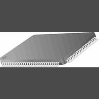
PC87393VJG National Semiconductor, PC87393VJG Datasheet - Page 121

PC87393VJG
Manufacturer Part Number
PC87393VJG
Description
IC, SUPER I/O DEVICE, TQFP-100
Manufacturer
National Semiconductor
Specifications of PC87393VJG
Data Rate
2Mbps
Supply Voltage Range
3V to 3.6V
Logic Case Style
TQFP
No. Of Pins
100
Operating Temperature Range
0°C to +70°C
Termination Type
SMD
Transceiver Type
Interface
Rohs Compliant
No
Available stocks
Company
Part Number
Manufacturer
Quantity
Price
Part Number:
PC87393VJG
Manufacturer:
NS/国半
Quantity:
20 000
- Current page: 121 of 148
- Download datasheet (703Kb)
www.national.com
8.0 Legacy Functional Blocks
This chapter briefly describes the following blocks that provide legacy device functions:
The description of each Legacy block includes the sections listed below. For details on the general implementation of each
legacy block, see the SuperI/O Legacy Functional Blocks datasheet.
The register maps in this chapter use the following abbreviations for Type:
8.1 FLOPPY DISK CONTROLLER (FDC)
8.1.1
The generic FDC is a standard FDC with a digital data separator, and is DP8473 and N82077 software compatible.
The FDC is implemented in this device as follows:
8.1.2
Floppy Disk Controller (FDC)
Parallel Port
Serial Port 1 (SP1), UART Functionality for both Serial Port 1 and Serial Port 2
Serial Port 2 (SP2), Infrared Functionality
General Description
Register Map table(s)
Bitmap table(s).
R/W = Read/Write
R = Read from a specific address returns the value of a specific register. Write to the same address is to a different
register.
W = Write
RO = Read Only
R/W1C = Read/Write 1 to Clear. Writing 1 to a bit clears it to 0. Writing 0 has no effect.
FM and MFM modes are supported. To select either mode, set bit 6 of the first command byte when writing to/read-
ing from a diskette, where:
0 = FM mode
1 = MFM mode
Automatic media sense is supported by MSEN1-0 pins only on FDC signals routed to the PPM functional block (on
the Parallel Port).
DRATE1 is not supported.
A logic 1 is returned for all floating (TRI-STATE) FDC register bits upon LPC I/O read cycles.
General Description
FDC Register Map
Offset
00h
01h
02h
03h
04h
05h
06h
07h
Mnemonic
FIFO
DOR
MSR
DSR
CCR
SRA
SRB
TDR
DIR
Status A
Status B
Digital Output
Tape Drive
Main Status
Data Rate Select
Data (FIFO)
Digital Input
Configuration Control
121
Register Name
Reserved
Type
R/W
R/W
R/W
RO
RO
W
W
R
R
Related parts for PC87393VJG
Image
Part Number
Description
Manufacturer
Datasheet
Request
R
Part Number:
Description:
National Semiconductor [8-Bit D/A Converter]
Manufacturer:
National Semiconductor
Datasheet:
Part Number:
Description:
National Semiconductor [Media Coprocessor]
Manufacturer:
National Semiconductor
Datasheet:
Part Number:
Description:
Digitally Controlled Tone and Volume Circuit with Stereo Audio Power Amplifier, Microphone Preamp Stage and National 3D Sound
Manufacturer:
National Semiconductor
Datasheet:
Part Number:
Description:
Digitally Controlled Tone and Volume Circuit with Stereo Audio Power Amplifier, Microphone Preamp Stage and National 3D Sound
Manufacturer:
National Semiconductor
Datasheet:
Part Number:
Description:
AC97 Rev 2 Codec with Sample Rate Conversion and National 3D Sound
Manufacturer:
National Semiconductor
Part Number:
Description:
Manufacturer:
National Semiconductor
Datasheet:
Part Number:
Description:
Manufacturer:
National Semiconductor
Datasheet:
Part Number:
Description:
General Purpose, Low Voltage, Low Power, Rail-to-Rail Output Operational Amplifiers
Manufacturer:
National Semiconductor
Datasheet:
Part Number:
Description:
8-bit 20 MSPS flash A/D converter.
Manufacturer:
National Semiconductor
Datasheet:
Part Number:
Description:
Low Noise Quad Operational Amplifier
Manufacturer:
National Semiconductor
Datasheet:
Part Number:
Description:
Quad Differential Line Receivers
Manufacturer:
National Semiconductor
Datasheet:
Part Number:
Description:
Quad High Speed Trapezoidal? Bus Transceiver
Manufacturer:
National Semiconductor
Datasheet:
Part Number:
Description:
Dual Line Receiver
Manufacturer:
National Semiconductor
Datasheet:
Part Number:
Description:
TTL to 10k ECL Level Translator with Latch
Manufacturer:
National Semiconductor
Datasheet:


