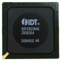
IDT82P2821BHG IDT, Integrated Device Technology Inc, IDT82P2821BHG Datasheet - Page 118

IDT82P2821BHG
Manufacturer Part Number
IDT82P2821BHG
Description
IC LINE INTERFACE UNIT 640-PBGA
Manufacturer
IDT, Integrated Device Technology Inc
Datasheet
1.IDT82P2821BHG.pdf
(151 pages)
Specifications of IDT82P2821BHG
Function
Line Interface Unit (LIU)
Interface
E1, J1, T1
Number Of Circuits
1
Voltage - Supply
1.8V, 3.3V
Operating Temperature
-40°C ~ 85°C
Mounting Type
Surface Mount
Package / Case
*
Includes
Defect and Alarm Detection, Driver Over-Current Detection and Protection, LLOS Detection, PRBSARB / IB Detection and Generation
Number Of Transceivers
1
Screening Level
Industrial
Mounting
Surface Mount
Operating Temperature (min)
-40C
Operating Temperature (max)
85C
Lead Free Status / RoHS Status
Lead free / RoHS Compliant
Current - Supply
-
Power (watts)
-
Lead Free Status / RoHS Status
Compliant, Lead free / RoHS Compliant
Other names
800-1703
82P2821BHG
82P2821BHG
Available stocks
Company
Part Number
Manufacturer
Quantity
Price
Company:
Part Number:
IDT82P2821BHG
Manufacturer:
IDT
Quantity:
170
Company:
Part Number:
IDT82P2821BHG
Manufacturer:
IDT, Integrated Device Technology Inc
Quantity:
10 000
6
as described in the IEEE 1149.1 standards.
registers plus a Test Access Port (TAP) controller. The control of the TAP
is achieved through signals applied to the Test Mode Select (TMS) and
Test Clock (TCK) input pins. Data is shifted into the registers via the Test
6.1
executed or the data register to be accessed or both.
BYPASS, CLAMP and HIGHZ.
6.2
6.2.1
Manufacturer Identity and a fixed bit.
6.2.2
the TDI input and the TDO output. Bypassing the BYR will reduce test
access times.
JTAG
IDT82P2821
The IDT82P2821 supports the digital Boundary Scan Specification
The boundary scan architecture consists of data and instruction
The IR with instruction decode block is used to select the test to be
The instructions include: EXTEST, SAMPLE/PRELOAD, IDCODE,
The IDR can be set to define the Version, the Part Number, the
The BYP consists of a single bit. It can provide a serial path between
JTAG
JTAG INSTRUCTION REGISTER (IR)
JTAG DATA REGISTER
DEVICE IDENTIFICATION REGISTER (IDR)
BYPASS REGISTER (BYP)
TRST
TMS
TCK
TDI
Port) Controller
(Test Access
TAP
DIR (Device Identification Register)
BSR (Boundary Scan Register)
IR (Instruction Register)
BR (Bypass Register)
Figure-49 JTAG Architecture
Control
21(+1) CHANNEL HIGH-DENSITY T1/E1/J1 LINE INTERFACE UNIT
118
Data Input (TDI) pin, and shifted out of the registers via the Test Data
Output (TDO) pin. Both TDI and TDO are clocked at a rate determined
by TCK.
Register), DIR (Device Identification Register), BR (Bypass Register)
and IR (Instruction Register). These will be described in the following
pages. Refer to Figure-49 for architecture.
6.2.3
6.3
states include: Test Logic Reset, Run-Test/Idle, Select-DR-Scan,
Capture-DR, Shift-DR, Exit1-DR, Pause-DR, Exit2-DR, Update-DR,
Select-IR-Scan, Capture-IR, Shift-IR, Exit1-IR, Pause-IR, Exit2-IR and
Update-IR.
main branches to access either the data or instruction registers. The
value shown next to each state transition in this figure states the value
present at TMS at each rising edge of TCK.
The bidirectional ports interface to 2 boundary scan cells:
The TAP controller is a 16-state synchronous state machine. The
Figure-50 shows the state diagram. Note that the figure contains two
The JTAG boundary scan registers include BSR (Boundary Scan
- In cell: The input cell is observable only.
- Out cell: The output cell is controllable and observable.
TEST ACCESS PORT (TAP) CONTROLLER
BOUNDARY SCAN REGISTER (BSR)
Output Enable
Select
MUX
February 6, 2009
TDO


