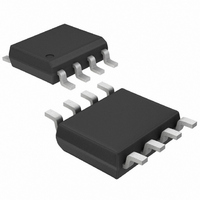
MAX4364ESA+ Maxim Integrated Products, MAX4364ESA+ Datasheet - Page 12

MAX4364ESA+
Manufacturer Part Number
MAX4364ESA+
Description
IC AMP AUDIO PWR 1.4W MONO 8SOIC
Manufacturer
Maxim Integrated Products
Type
Class ABr
Datasheet
1.MAX4364ESA.pdf
(15 pages)
Specifications of MAX4364ESA+
Output Type
1-Channel (Mono)
Max Output Power X Channels @ Load
1.4W x 1 @ 8 Ohm
Voltage - Supply
2.7 V ~ 5.5 V
Features
Depop, Short-Circuit and Thermal Protection, Shutdown
Mounting Type
Surface Mount
Package / Case
8-SOIC (3.9mm Width)
Package
8SOIC N
Function
Speaker
Amplifier Type
Class-AB
Total Harmonic Distortion Noise
0.04@8Ohm@1000mW %
Typical Psrr
75 dB
Output Signal Type
Differential
Maximum Load Resistance
8 Ohm
Product
General Purpose Audio Amplifiers
Output Power
1.4 W
Thd Plus Noise
0.04 %
Supply Current
7 mA
Maximum Power Dissipation
471 mW
Maximum Operating Temperature
+ 85 C
Mounting Style
SMD/SMT
Audio Load Resistance
8 Ohms
Minimum Operating Temperature
- 40 C
Amplifier Class
AB
No. Of Channels
1
Supply Voltage Range
2.7V To 5.5V
Load Impedance
8ohm
Operating Temperature Range
-40°C To +85°C
Amplifier Case Style
SOIC
Rohs Compliant
Yes
Lead Free Status / RoHS Status
Lead free / RoHS Compliant
1.4W and 1W, Ultra-Small, Audio Power
Amplifiers with Shutdown
Proper selection of AC-coupling capacitors (C
C
The value of C
midrail bias voltage rises on startup and falls when enter-
ing shutdown. The size of the input capacitor also affects
clickless/popless operation. On startup, C
to its quiescent DC voltage through the feedback resistor
(R
sient at the amplifier’s output, which can result in an
audible pop. Minimizing the size of C
effect, optimizing click-and-pop suppression.
Proper supply bypassing ensures low-noise, low-distor-
tion performance. Place a 0.1µF ceramic capacitor in
parallel with a 10µF ceramic capacitor from V
GND. Locate the bypass capacitors as close to the
device as possible.
The addition of a digital potentiometer provides simple
volume control. Figure 3 shows the MAX4364/MAX4365
with the MAX5407 log taper digital potentiometer used
as an input attenuator. Connect the high terminal of the
MAX5407 to the audio input, the low terminal to ground
and the wiper to C
12
BIAS
F
) from the output. This current creates a voltage tran-
______________________________________________________________________________________
TOP VIEW
achieves clickless/popless shutdown and startup.
SHDN
BIAS
BIAS
GND
BIAS
IN+
IN+
IN-
IN-
IN
1
2
4
1
2
4
3
3
. Setting the wiper to the top posi-
determines the rate at which the
MAX/TDFN
MAX4364
MAX4365
Pin Configurations
Clickless/Popless Operation
Adding Volume Control
SO
6
6
8
7
5
8
7
5
Supply Bypassing
OUT-
V
OUT-
SHDN
V
OUT+
GND
OUT+
CC
CC
IN
IN
reduces this
is charged
IN
CC
) and
to
tion passes the audio signal unattenuated. Setting the
wiper to the lowest position fully attenuates the input.
Good layout improves performance by decreasing the
amount of stray capacitance and noise at the amplifier’s
inputs and outputs. Decrease stray capacitance by min-
imizing PC board trace lengths, using surface-mount
components and placing external components as close
to the device as possible. Also refer to the Power
Dissipation section for heatsinking considerations.
Figure 3. MAX4364/MAX4365 and MAX5160 Volume Control
Circuit
MAX4364 TRANSISTOR COUNT: 772
MAX4365 TRANSISTOR COUNT: 768
PROCESS: BiCMOS
AUDIO
INPUT
1 H
4 L
MAX5407
W 3
C
IN
R
IN
Layout Considerations
Chip Information
IN-
MAX4364
MAX4365
R
F
OUT+
OUT-


