LM4856LQ/NOPB National Semiconductor, LM4856LQ/NOPB Datasheet
LM4856LQ/NOPB
Specifications of LM4856LQ/NOPB
LM4856LQTR


Related parts for LM4856LQ/NOPB

LM4856LQ/NOPB Summary of contents
Page 1
... Typical Application FIGURE 1. Typical Audio Amplifier Application Circuit Boomer ® registered trademark of National Semiconductor Corporation. © 2004 National Semiconductor Corporation Key Specifications n THD+N at 1kHz, 1.1W into 8Ω BTL n THD+N at 1kHz, 60mW into 32Ω Single Supply Operation Features n 1.1W (typ) output power with 8Ω ...
Page 2
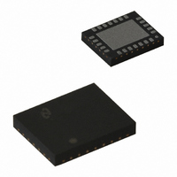
Connection Diagrams Top View (Bump-side down) Order Number LM4856ITL See NS Package Number TLA18AAA LLP Package Top View Order Number LM4856LQ See NS Package Number LQA24A for Exposed-DAP LLP www.national.com 18-Bump micro SMD Marking (ITL) 200607A9 Z - Assembly Plant ...
Page 3
... Absolute Maximum Ratings If Military/Aerospace specified devices are required, please contact the National Semiconductor Sales Office/ Distributors for availability and specifications. Supply Voltage Storage Temperature ESD Susceptibility (Note 4) ESD Machine model (Note 7) Junction Temperature ( Solder Information (Note 1) Vapor Phase (60 sec.) Infrared (15 sec.) ...
Page 4
Electrical Characteristics The following specifications apply for V Symbol Parameter V Logic Low Input Voltage IL Digital Volume Range (R and Digital Volume Range (Phone_In_HS) Digital Volume Stepsize Digital Volume Stepsize Error Phone_In_IHF Volume Phone_In_IHF Mute ...
Page 5
Electrical Characteristics The following specifications apply for V Symbol Parameter I Supply Current DD I Shutdown Current SD V Output Offset Voltage OS P Output Power O Total Harmonic Distortion Plus THD+N Noise N Output Noise OUT Power Supply Rejection ...
Page 6
Electrical Characteristics The following specifications apply for V Symbol Parameter Digital Volume Range (R and Digital Volume Range (Phone_In_HS) Digital Volume Stepsize Digital Volume Stepsize Error Phone_In_IHF Volume Phone _In_IHF Mute Attenuation Phone_In_IHF Input Impedance Phone_In_HS ...
Page 7
External Components Description Components 1. C This is the input coupling capacitor. It blocks the DC voltage and couples the input signal to the amplifier’s IN input terminals 1/(2π This is the ...
Page 8
Typical Performance Characteristics THD+N vs Frequency THD+N vs Frequency THD+N vs Frequency www.national.com (Continued) THD+N vs Frequency 200607G7 THD+N vs Frequency 200607B5 THD+N vs Frequency 200607H0 8 200607G8 200607G9 200607H1 ...
Page 9
Typical Performance Characteristics THD+N vs Output Power LM4856LQ THD+N vs Output Power THD+N vs Output Power (Continued) THD+N vs Output Power 200607F2 THD+N vs Output Power 200607B9 THD+N vs Output Power 200607C1 9 LM4856LQ 200607F3 200607H2 200607H3 www.national.com ...
Page 10
Typical Performance Characteristics Power Supply Rejection Ratio Power Supply Rejection Ratio Power Supply Rejection Ratio www.national.com (Continued) Power Supply Rejection Ratio 200607C3 Power Supply Rejection Ratio 200607C5 Power Supply Rejection Ratio 200607C7 10 200607H4 200607H5 200607H6 ...
Page 11
Typical Performance Characteristics Output Power vs Supply Voltage Output Power vs Load Resistance Power Dissipation vs Output Power (Continued) Output Power vs Supply Voltage 200607D7 Output Power vs Load Resistance 200607D9 Power Dissipation vs Output Power 200607E1 11 200607H7 200607H8 ...
Page 12
Typical Performance Characteristics Supply Current vs Supply Voltage Frequency Response www.national.com (Continued) Channel Separation 200607C9 Frequency Response 200607D4 Frequency Response 200607I1 12 200607I2 200607I0 ...
Page 13
Typical Performance Characteristics Output Mode gain from gain from LIN/RIN to LOUT/ROUT A - weighted filter used (Continued) Output Noise vs Output Mode (V = 3V, 5V) DD ...
Page 14
Application Information PIN DESCRIPTION SDA: This is the serial data input pin. SCL: This is the clock input pin. ADR: This is the address select input pin INTERFACE The LM4856 uses a serial bus, ...
Page 15
Application Information BIT D7 D6 Function Name V4 V3 Default Handsfree Speaker Output 12dB x P IHF MUTE 12dB x P IHF ...
Page 16
Application Information ...
Page 17
... LM4856’s thermal shutdown protection. Further detailed and specific information con- cerning PCB layout and fabrication and mounting an LD (LLP) is found in National Semiconductor’s AN1187. PCB LAYOUT AND SUPPLY REGULATION CONSIDERATIONS FOR DRIVING 3Ω AND 4Ω LOADS Power dissipated by a load is a function of the voltage swing across the load and the load’ ...
Page 18
Application Information temperature that still allows maximum stereo power dissipa- tion without violating the LM4856’s maximum junction tem- perature JMAX DMAX-TOTAL For a typical application with a 5V power supply and an 8Ω load, ...
Page 19
Demonstration ITL/LQ Board Layout Recommended ITL PC Board Layout: Top Overlay Layer Recommended ITL PC Board Layout: Middle 1 Layer 200607G0 Recommended ITL PC Board Layout: 200607F7 Recommended ITL PC Board Layout: Middle 2 Layer 19 200607F9 Top Layer 200607F8 ...
Page 20
Demonstration ITL/LQ Board Layout Recommended ITL PC Board Layout: Bottom Layer Recommended LQ PC Board Layout: Top Layer www.national.com (Continued) 200607F6 Recommended LQ PC Board Layout: Top Overlay Layer 200607G4 Recommended LQ PC Board Layout: Middle 1 Layer 20 200607G5 ...
Page 21
Demonstration ITL/LQ Board Layout Recommended LQ PC Board Layout: Middle 2 Layer (Continued) 200607G3 Recommended LQ PC Board Layout: Bottom Layer 21 200607G1 www.national.com ...
Page 22
Physical Dimensions 24-Lead MOLDED PKG, Leadless Leadframe Package LLP www.national.com inches (millimeters) unless otherwise noted Order Number LM4856LQ NS Package Number LQA24A 22 ...
Page 23
... BANNED SUBSTANCE COMPLIANCE National Semiconductor certifies that the products and packing materials meet the provisions of the Customer Products Stewardship Specification (CSP-9-111C2) and the Banned Substances and Materials of Interest Specification (CSP-9-111S2) and contain no ‘‘Banned Substances’’ as defined in CSP-9-111S2. ...