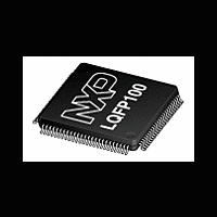
LPC2387FBD100 NXP Semiconductors, LPC2387FBD100 Datasheet - Page 33

LPC2387FBD100
Manufacturer Part Number
LPC2387FBD100
Description
The LPC2387 is an ARM7 microcontroller for embedded applications featuring a high level of integration and low power consumption at frequencies of 72 MHz
Manufacturer
NXP Semiconductors
Datasheet
1.LPC2387FBD100.pdf
(66 pages)
Available stocks
Company
Part Number
Manufacturer
Quantity
Price
Company:
Part Number:
LPC2387FBD100
Manufacturer:
NXP
Quantity:
3 000
Part Number:
LPC2387FBD100
Manufacturer:
NXP/恩智浦
Quantity:
20 000
Company:
Part Number:
LPC2387FBD100,551
Manufacturer:
NXP Semiconductors
Quantity:
10 000
NXP Semiconductors
LPC2387
Product data sheet
7.25.5 External interrupt inputs
7.25.6 Memory mapping control
7.26.1 EmbeddedICE
7.26.2 Embedded trace
7.26 Emulation and debugging
The second AHB, referred to as AHB2, includes only the Ethernet block and an
associated 16 kB SRAM. In addition, a bus bridge is provided that allows the secondary
AHB to be a bus master on AHB1, allowing expansion of Ethernet buffer space into
unused space in memory residing on AHB1.
In summary, bus masters with access to AHB1 are the ARM7 itself, the USB block, the
GPDMA function, and the Ethernet block (via the bus bridge from AHB2). Bus masters
with access to AHB2 are the ARM7 and the Ethernet block.
The LPC2387 include up to 46 edge sensitive interrupt inputs combined with up to four
level sensitive external interrupt inputs as selectable pin functions. The external interrupt
inputs can optionally be used to wake up the processor from Power-down mode.
The memory mapping control alters the mapping of the interrupt vectors that appear at the
beginning at address 0x0000 0000. Vectors may be mapped to the bottom of the Boot
ROM or the SRAM. This allows code running in different memory spaces to have control
of the interrupts.
The LPC2387 supports emulation and debugging via a JTAG serial port. A trace port
allows tracing program execution. Debugging and trace functions are multiplexed only
with GPIOs on P2[0] to P2[9]. This means that all communication, timer, and interface
peripherals residing on other pins are available during the development and debugging
phase as they are when the application is run in the embedded system itself.
The EmbeddedICE logic provides on-chip debug support. The debugging of the target
system requires a host computer running the debugger software and an EmbeddedICE
protocol convertor. The EmbeddedICE protocol convertor converts the Remote Debug
Protocol commands to the JTAG data needed to access the ARM7TDMI-S core present
on the target system.
The ARM core has a Debug Communication Channel (DCC) function built-in. The DCC
allows a program running on the target to communicate with the host debugger or another
separate host without stopping the program flow or even entering the debug state. The
DCC is accessed as a co-processor 14 by the program running on the ARM7TDMI-S
core. The DCC allows the JTAG port to be used for sending and receiving data without
affecting the normal program flow. The DCC data and control registers are mapped in to
addresses in the EmbeddedICE logic.
The JTAG clock (TCK) must be slower than
interface to operate.
Since the LPC2387 has significant amounts of on-chip memories, it is not possible to
determine how the processor core is operating simply by observing the external pins. The
ETM provides real-time trace capability for deeply embedded processor cores. It outputs
All information provided in this document is subject to legal disclaimers.
Rev. 5 — 9 January 2012
1
⁄
6
of the CPU clock (CCLK) for the JTAG
Single-chip 16-bit/32-bit MCU
LPC2387
© NXP B.V. 2012. All rights reserved.
33 of 66


