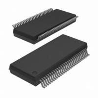
74ALVT16652DL,518 NXP Semiconductors, 74ALVT16652DL,518 Datasheet - Page 7

74ALVT16652DL,518
Manufacturer Part Number
74ALVT16652DL,518
Description
IC 16BIT BUS TXRX 3-ST 56SSOP
Manufacturer
NXP Semiconductors
Series
74ALVTr
Datasheet
1.74ALVT16652DGG118.pdf
(14 pages)
Specifications of 74ALVT16652DL,518
Logic Type
Transceiver, Non-Inverting
Number Of Elements
2
Number Of Bits Per Element
8
Current - Output High, Low
8mA, 24mA
Voltage - Supply
2.3 V ~ 2.7 V, 3 V ~ 3.6 V
Operating Temperature
-40°C ~ 85°C
Mounting Type
Surface Mount
Package / Case
56-SSOP
Lead Free Status / RoHS Status
Lead free / RoHS Compliant
Other names
74ALVT16652DL-T
74ALVT16652DL-T
935209980518
74ALVT16652DL-T
935209980518
1. All typical values are at V
2. This is the increase in supply current for each input at the specified voltage level other than V
3. This parameter is valid for any V
4. Unused pins at V
5. I
6. For valid test results, data must not be loaded into the flip-flops (or latches) after applying power.
7. This is the bus hold overdrive current required to force the input to the opposite logic state.
Philips Semiconductors
DC ELECTRICAL CHARACTERISTICS (3.3V "0.3V RANGE)
GND = 0V; t
NOTES:
1998 Feb 13
SYMBOL
2.5V/3.3V 16-bit bus transceiver/register
(3-State)
I
transition time of 100 sec is permitted. This parameter is valid for T
I
V
PU/PD
HOLD
I
CCZ
V
V
I
I
I
V
V
V
OFF
I
CCH
CCL
CCZ
RST
EX
I
OH
OH
OL
OL
I
CC
IK
I
is measured with outputs pulled up to V
R
= t
Input clamp voltage
High-level output voltage
High-level out ut voltage
Low–level output voltage
Low–level out ut voltage
Power-up output low voltage
Input leakage current
Off current
Bus Hold current
Bus Hold current
Data inputs
Data in uts
Current into an output in the
High state when V
Power up/down 3-State output
current
Quiescent supply current
Additional supply current per
input pin
F
= 2.5ns; C
CC
3
2
PARAMETER
or GND.
7
CC
L
= 50pF; R
= 3.3V and T
O
> V
CC
CC
between 0V and 1.2V with a transition time of up to 10msec. From V
L
= 500 ; T
6
amb
CC
V
V
V
V
V
V
V
V
V
V
V
V
V
V
V
V
V
V
V
OE/OE = Don’t care
V
V
V
V
Other inputs at V
= 25 C.
CC
CC
CC
CC
CC
CC
CC
CC
CC
CC
CC
CC
CC
CC
CC
CC
CC
O
CC
CC
CC
CC
CC
or pulled down to ground.
= 5.5V; V
amb
= 3.0V; I
= 3.0 to 3.6V; I
= 3.0V; I
= 3.0V; I
= 3.0V; I
= 3.0V; I
= 3.0V; I
= 3.6V; I
= 3.6V; V
= 0 or 3.6V; V
= 3.6V; V
= 3.6V; V
= 3.6V; V
= 0V; V
= 3V; V
= 3V; V
= 3.0V; V
= 3.6V; Outputs High, V
= 3.6V; Outputs Low, V
= 3.6V; Outputs Disabled; V
= 3V to 3.6V; One input at V
1.2V; V
= –40 C to +85 C.
I
I
I
CC
IK
OH
OL
OL
OL
OL
O
or V
= 0.8V
= 2.0V
O
I
I
I
I
I
= 1mA; V
= V
= 5.5V
= V
= 0
= 0V to 3.6V
= –18mA
= 0.5V to V
= 3.0V
= 100 A
= 16mA
= 32mA
= 64mA
= –32mA
CC
O
TEST CONDITIONS
I
CC
CC
OH
= 0 to 4.5V
= 5.5V
or GND
or GND
= –100 A
7
amb
I
= V
CC
I
= 25 C only.
I
CC
= GND or V
= GND or V
; V
or GND
I
I
CC
= GND or V
= GND or V
–0.6V,
CC,
CC,
I/O Data pins
Control pins
Control ins
I
I
O =
CC
CC,
O =
CC
0
0
I
O =
or GND
0
5
4
V
CC
Temp = -40 C to +85 C
CC
MIN
–75
2.0
75
500
= 1.2V to V
–0.2
74ALVT16652
LIMITS
–0.85
TYP
–140
V
0.07
0.25
0.07
0.07
0.04
130
2.3
0.3
0.4
0.1
0.1
0.1
0.5
0.1
0.1
3.2
50
40
CC
CC
1
Product specification
= 3.3V
MAX
–1.2
0.55
0.55
0.14
0.14
125
0.2
0.4
0.5
0.4
10
20
10
100
100
-5
7
1
0.3V a
UNIT
mA
mA
V
V
V
V
V
V
A
A
A
A
A
A
A


