HCF40193BEY STMicroelectronics, HCF40193BEY Datasheet
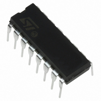
IC COUNTER PRESET UP/DOWN 16-DIP

HCF40193BEY

Manufacturer Part Number
HCF40193BEY
Description
IC COUNTER PRESET UP/DOWN 16-DIP
Manufacturer
STMicroelectronics
Series
4000Br
Datasheet

Specifications of HCF40193BEY

Logic Type
Binary Counter
Direction
Up, Down
Number Of Elements
1
Number Of Bits Per Element
4
Reset
Asynchronous
Timing
Synchronous
Count Rate
11MHz
Trigger Type
Positive Edge
Voltage - Supply
3 V ~ 20 V
Operating Temperature
-55°C ~ 125°C
Mounting Type
Through Hole
Package / Case
16-DIP (0.300", 7.62mm)
Lead Free Status / RoHS Status
Lead free / RoHS Compliant

Available stocks

Company
Part Number
Manufacturer
Quantity
Price
Part Number:
HCF40193BEY
Manufacturer:
ST
0
DESCRIPTION
HCF40193B is a monolithic integrated circuit
fabricated
technology available in DIP and SOP packages.
HCF40193B Presettable Binary Up/Down Counter
consists of 4 synchronously clocked, GATED "D"
type flip-flops connected as a counter. The inputs
consist of four individual jam lines, a PRESET
ENABLE control, individual CLOCK UP and
CLOCK DOWN signals and a master RESET.
Four buffered Q signal outputs as well as CARRY
PIN CONNECTION
September 2002
INDIVIDUAL CLOCK LINES FOR COUNTING
UP OR COUNTING DOWN
SYNCHRONOUS HIGH-SPEED CARRY AND
BORROW PROPAGATION DELAYS FOR
CASCADING
ASYNCHRONOUS RESET AND PRESET
CAPABILITY
MEDIUM-SPEED OPERATION - f
(typ.) AT 10 V
STANDARDIZED SYMMETRICAL OUTPUT
CHARACTERISTICS
QUIESCENT CURRENT SPECIF. UP TO 20V
5V, 10V AND 15V PARAMETRIC RATINGS
INPUT LEAKAGE CURRENT
I
100% TESTED FOR QUIESCENT CURRENT
MEETS ALL REQUIREMENTS OF JEDEC
JESD13B "STANDARD SPECIFICATIONS
FOR DESCRIPTION OF B SERIES CMOS
DEVICES"
I
= 100nA (MAX) AT V
in
Metal
Oxide
DD
= 18V T
(DUAL CLOCK WITH RESET) BINARY TYPE
Semiconductor
A
CL
PRESETTABLE UP/DOWN COUNTERS
= 25°C
= 8MHz
ORDER CODES
and BORROW outputs for multiple-stage counting
schemes are provided. The counter is cleared so
that all outputs are in a low state by a high on the
RESET
asynchronously with the clock. Each output is
individually programmable asynchronously with
the clock to the level on the corresponding jam
input when the PRESET ENABLE control is low.
The counter counts up one count on the positive
clock edge of the CLOCK UP signal provided the
CLOCK DOWN line is high. The counter counts
down one count on the positive clock edge of the
CLOCK DOWN signal provided the CLOCK UP
line is high. The CARRY and BORROW signals
are high when the counter counts up or down. The
CARRY signal goes low one-half clock cycle after
the counter reaches its maximum count in the
count-up mode. The BORROW signal goes low
PACKAGE
SOP
DIP
line.
DIP
HCF40193BM1
HCF40193BEY
A
TUBE
RESET
HCF40193B
HCF40193M013TR
is
SOP
accomplished
T & R
1/12

Related parts for HCF40193BEY

HCF40193BEY Summary of contents

Page 1

... The CARRY signal goes low one-half clock cycle after the counter reaches its maximum count in the count-up mode. The BORROW signal goes low HCF40193B DIP SOP TUBE T & R HCF40193BEY HCF40193BM1 HCF40193M013TR A RESET is accomplished 1/12 ...

Page 2

HCF40193B one-half clock cycle after the counter reaches its minimum count in the count-down mode. The cascading of multiple packages accomplished without the need for additional IINPUT EQUIVALENT CIRCUIT FUNCTIONAL DIAGRAM 2/12 external circuitry by tying the BORROW and CARRY ...

Page 3

LOGIC DIAGRAM TRUTH TABLE CLOCK UP CLOCK DOWN (X) : Don’t Care PRESET ENABLE HCF40193B RESET ACTION L COUNT COUNT L COUNT DOWN ...

Page 4

HCF40193B TIMING DIAGRAM INTERNAL LOGIG OF FLIP-FLOP 4/12 ...

Page 5

ABSOLUTE MAXIMUM RATINGS Symbol V Supply Voltage Input Voltage Input Current I P Power Dissipation per Package D Power Dissipation per Output Transistor T Operating Temperature op T Storage Temperature stg Absolute Maximum Ratings ...

Page 6

HCF40193B DC SPECIFICATIONS Symbol Parameter V (V) I Quiescent Current 0/5 L 0/10 0/15 0/20 V High Level Output 0/5 OH Voltage 0/10 0/15 V Low Level Output 5/0 OL Voltage 10/0 15/0 V High Level Input IH Voltage V ...

Page 7

DYNAMIC ELECTRICAL CHARACTERISTICS (T Symbol Parameter t t Propagation Delay Time PLH PHL Clock Up or Clock Down to Q Reset Clock Up to Carry Clock Down to Borrow Reset Borrow or ...

Page 8

HCF40193B TEST CIRCUIT C = 50pF or equivalent (includes jig and probe capacitance 200K pulse generator (typically OUT WAVEFORM 1 : PROPAGATION DELAY TIMES (f=1MHz; 50% duty cycle) 8/12 ...

Page 9

WAVEFORM 2 : MINIMUM PULSE WIDTH AND REMOVAL TIME (f=1MHz; 50% duty cycle) TYPICAL APPLICATION: CASCADED COUNTER PACKAGES HCF40193B 9/12 ...

Page 10

HCF40193B Plastic DIP-16 (0.25) MECHANICAL DATA DIM. MIN. a1 0. 10/12 mm. TYP MAX. MIN. 0.020 1.65 0.030 0.5 0.25 20 8.5 2.54 17.78 7.1 5.1 3.3 1.27 ...

Page 11

SO-16 MECHANICAL DATA mm. DIM. MIN. TYP 0.35 b1 0. 9.8 E 5.8 e 1.27 e3 8.89 F 3.8 G 4 inch MAX. MIN. TYP. 1.75 0.2 ...

Page 12

... No license is granted by implication or otherwise under any patent or patent rights of STMicroelectronics. Specifications mentioned in this publication are subject to change without notice. This publication supersedes and replaces all information previously supplied ...

Related keywords