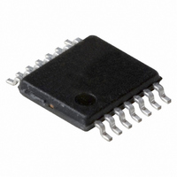
74HC73DB,112 NXP Semiconductors, 74HC73DB,112 Datasheet - Page 8

74HC73DB,112
Manufacturer Part Number
74HC73DB,112
Description
IC DUAL JK FF NEG-EDGE 14-SSOP
Manufacturer
NXP Semiconductors
Series
74HCr
Type
JK Typer
Datasheet
1.74HC73N652.pdf
(16 pages)
Specifications of 74HC73DB,112
Output Type
Differential
Package / Case
14-SSOP
Function
Reset
Number Of Elements
2
Number Of Bits Per Element
1
Frequency - Clock
77MHz
Delay Time - Propagation
15ns
Trigger Type
Negative Edge
Current - Output High, Low
5.2mA, 5.2mA
Voltage - Supply
2 V ~ 6 V
Operating Temperature
-40°C ~ 125°C
Mounting Type
Surface Mount
Number Of Circuits
2
Logic Family
HC
Logic Type
J-K Negative Edge Triggered Flip Flop
Polarity
Inverting/Non-Inverting
Input Type
Single-Ended
Propagation Delay Time
16 ns at 5 V
High Level Output Current
- 5.2 mA
Low Level Output Current
5.2 mA
Supply Voltage (max)
6 V
Maximum Operating Temperature
+ 125 C
Mounting Style
SMD/SMT
Minimum Operating Temperature
- 40 C
Supply Voltage (min)
2 V
Lead Free Status / RoHS Status
Lead free / RoHS Compliant
Lead Free Status / RoHS Status
Lead free / RoHS Compliant, Lead free / RoHS Compliant
Other names
568-2736-5
935190270112
935190270112
Available stocks
Company
Part Number
Manufacturer
Quantity
Price
Company:
Part Number:
74HC73DB,112
Manufacturer:
IDT
Quantity:
123
NXP Semiconductors
11. Waveforms
74HC73_4
Product data sheet
Fig 6.
Fig 7.
The shaded areas indicate when the input is permitted to change for predictable output performance.
Measurement points are given in
V
Waveforms showing the clock (nCP) to output (nQ, nQ) propagation delays, the clock pulse width, the J
and K to nCP set-up and hold times, the output transition times and the maximum clock frequency
Measurement points are given in
V
Waveforms showing the reset (nR) input to output (nQ, nQ) propagation delays and the reset pulse width
and the nR to nCP removal time
OL
OL
and V
and V
OH
OH
are typical voltage output levels that occur with the output load.
are typical voltage output levels that occur with the output load.
nQ output
nQ output
nJ, nK
input
nCP input
GND
GND
V
V
V
V
OH
OH
OL
OL
V
V
I
I
nQ output
nCP input
nR input
nQ output
Table
Table
GND
GND
V
V
V
V
V
8.
8.
M
OH
OH
OL
OL
V
V
t
su
I
I
Rev. 04 — 19 March 2008
V
M
t
t
90 %
10 %
PHL
PLH
90 %
t
t
h
t
PLH
W
1/f
V
V
10 %
M
M
V
t
t
max
THL
TLH
t
M
PHL
Dual JK flip-flop with reset; negative-edge trigger
t
W
t
su
t
rec
001aab984
t
t
10 %
PLH
PHL
t
h
V
M
001aab983
90 %
90 %
10 %
t
t
TLH
THL
© NXP B.V. 2008. All rights reserved.
74HC73
8 of 16


